Backscattered Electron Imaging Mechanics for Precision Electrode Slitting Tooling Selection
Backscattered electron imaging quantifies sub-micron carbide grain integrity and cobalt binder depletion to select slitting tools that prevent edge burrs.
Contrast

Signal Physics in Carbide Edge Inspection
Precision slitting tooling for lithium-ion battery electrodes depends on edge radius retention below 2.0 ± 0.5 μm across hundreds of thousands of cut meters. Tungsten carbide (WC-Co) circular rotary knives cut cathode active materials containing hard transition metal oxides. Detecting microscopic binder leaching, sub-surface micro-fracture, and cobalt-phase depletion requires characterization beyond topographical secondary electron detection.
Backscattered electron (BSE) imaging uses high-energy incident electrons that undergo elastic scattering with target atomic nuclei. Because the backscatter coefficient η increases monotonically with the atomic number Z of the target element, pure tungsten at 74 contrasts sharply with cobalt at 27 and carbon at 6. The resulting mean atomic number difference creates pronounced compositional contrast in solid-state quadrant detectors.
Secondary electron (SE) signals originate from inelastic scattering events within the top 5 to 50 nm of the specimen surface, highlighting roughness, grinding marks, and debris accumulation. Backscattered electrons emerge from an interaction volume reaching depths between 100 nm and 1.5 μm depending on beam accelerating voltage. Operating an annular BSE detector at 15 to 20 kV reveals subsurface micro-void coalescence, sub-micron cobalt binder pull-out, and early micro-crack paths beneath the polished tool rake face.
Inspecting an incoming rotary slitter knife via SE alone misses sub-surface phase agglomeration. BSE signals map the exact spatial distribution of the soft cobalt matrix holding the ultra-hard tungsten carbide grains together under cyclic shearing stresses.
A solid-state four-quadrant backscattered detector operating at 15 kV resolves cobalt binder depletion down to 50 nanometers beneath the ground bevel edge.
Knife edge durability correlates with the homogeneous dispersion of cobalt binder throughout the cemented carbide body. High backscatter yields from tungsten carbide grains appear bright in BSE micrographs, low-Z cobalt binder pools appear dark grey, and porosity or micro-cracks produce zero backscatter signal, registering as pure black regions. This direct Z-contrast mapping lets metrology technicians quantify cobalt mean free path and tungsten carbide grain size distributions without chemical etching.
Etchants alter delicate knife-edge geometry, whereas backscattered electron mechanics preserve edge topography while extracting compositional integrity.
Tooling wear during cathode slitting involves both mechanical abrasion and chemical degradation. Hard lithium nickel manganese cobalt oxide (NMC) particles abrade the cutting tip, while trace residual moisture and solvent residues accelerate binder oxidation. BSE imaging identifies the boundary between raw tool material degradation and electrode material transfer.
Aluminum current collector smear exhibits low Z-contrast relative to tungsten carbide, appearing as a dark surface layer that can be distinguished from carbide grain loss. An incoming inspection dossier based on quantitative compositional BSE micrographs separates manufacturing defects from operational wear mechanisms.
Carbide wear leads directly to burr formation along the slit electrode edge.

Scatter
Interaction Volumes and Penetration Dynamics
Quantifying edge degradation requires tuning electron beam acceleration voltage to match the microstructural dimensions of sub-micron tungsten carbide grades. The electron interaction volume follows the Kanaya-Okayama range equation, scaling inversely with material mass density. Cemented tungsten carbide slitting knives typically exhibit mass densities between 14.2 and 15.0 g/cm³ depending on cobalt binder mass fraction.
An incident electron beam set to 20 kV penetrates approximately 0.65 μm into a 6% cobalt carbide substrate. Setting the beam to 10 kV restricts the penetration depth to 0.18 μm, confining the backscatter emission to the immediate sub-surface zone of the knife apex.
Selecting appropriate accelerating voltages governs feature resolution during tooling audits. Excessive accelerating voltage expands the interaction volume laterally, blurring sub-micron binder paths between 0.4 μm tungsten carbide grains through beam spreading. Low accelerating voltages below 5 kV generate low backscatter coefficients, decreasing signal-to-noise ratios on high-speed solid-state diode detectors.
Precision knife audits utilize stepped voltage profiles: 10 kV for high-resolution edge profile integrity and 20 kV for subsurface stress-crack propagation analysis.
| Accelerating Voltage (kV) | Kanaya-Okayama Range (μm) | BSE Emission Depth (nm) | WC Phase Spatial Resolution (nm) | Cobalt Binder Resolution (nm) |
|---|---|---|---|---|
| 5.0 | 0.06 ± 0.01 | 18 ± 3 | 12 ± 2 | 8 ± 1 |
| 10.0 | 0.18 ± 0.02 | 55 ± 5 | 22 ± 3 | 15 ± 2 |
| 15.0 | 0.38 ± 0.04 | 115 ± 10 | 45 ± 5 | 32 ± 4 |
| 20.0 | 0.65 ± 0.06 | 195 ± 18 | 80 ± 8 | 60 ± 6 |
| 25.0 | 0.98 ± 0.09 | 290 ± 25 | 135 ± 12 | 95 ± 9 |
Backscattered electrons maintain anisotropic angular distributions following a cosine emission law relative to specimen surface normal vectors. When analyzing acute knife bevel angles ranging from 30° to 45°, tilted specimen stages distort backscatter collection efficiency across quadrant sensors. Topographical contrast components mix into the compositional signal when specimens remain perpendicular to the optic axis.
Specialized tooling holders tilt the cutting edge facet normal to the center of the annular detector, suppressing geometric shadowing while isolating atomic number variations.
Under ISO 18516 provisions for hardmetal microstructural examination, non-uniform cobalt pooling exceeding three mean grain diameters constitutes grounds for lot rejection.
Energy filtering grids on advanced in-lens BSE detectors isolate low-loss backscattered electrons. These electrons undergo single elastic events near the entry point, maintaining spatial information with negligible lateral spread. Low-loss filtering achieves spatial resolutions below 3 nm on ultra-fine carbide tooling.
This resolution exposes individual tungsten carbide grain boundary embrittlement before visible spalling occurs on the slitter edge.
Accelerating voltage choices ultimately define the detection window for microstructural anomalies.

Bevel
Knife Edge Geometries and Compositional Maps
Rotary slitting tools operate under severe compressive and shear loading during continuous foil slitting. Precision electrode production lines run at line speeds between 50 and 120 meters per minute, slitting double-sided coated current collectors. Anode copper foils range from 4.5 to 8.0 μm in thickness, coated with abrasive graphite and silicon-graphite compounds.
Cathode aluminum foils range from 10.0 to 15.0 μm, coated with lithium iron phosphate (LFP) or nickel-rich layered oxides (NMC811). The abrasive nature of dry cathode active materials induces mechanical micro-chipping along the slitter blade intersection line.
Backscattered electron analysis of worn blade bevels categorizes failure progressions into distinct physical mechanisms. Standard optical microscopy fails to distinguish active material compaction from parent tool material chipping. BSE imaging provides sharp compositional delineation.
Lithium cathode materials contain light elements such as carbon, oxygen, phosphorus, and aluminum, generating minimal backscatter intensity compared to the heavy tungsten carbide base matrix. Backscatter mapping shows active layer build-up on the tool rake face without requiring destructive cross-sectioning.
- Cobalt binder leaching manifests as dark interstitial voids between bright tungsten carbide grains along the acute cutting line.
- Tungsten carbide grain fracture appears as angular bright fragments detached from the tool substrate and embedded in the current collector cut edge.
- Adhesive foil smear presents as low-Z dark grey continuous patches adhering across the knife flank face.
- Thermal micro-cracking displays deep, black meandering fissures propagating perpendicular to the primary cutting direction across cobalt boundaries.
Measuring the cutting edge radius requires systematic high-magnification backscattered calibration. A fresh sub-micron grain size carbide tool demonstrates a tip radius between 0.8 and 1.5 μm. As continuous slitting progresses across 100,000 meters of cathode stock, the edge rounds to a radius exceeding 4.0 μm.
BSE imaging distinguishes symmetrical mechanical wear from asymmetrical chipping caused by side-clearance runout between upper and lower rotary knives. Asymmetrical wear patterns point to slitter spindle bearing runout rather than intrinsic carbide metallurgy deficiencies.
Sub-micron grain distributions significantly slow down edge rounding rates.
Stock
Grade Verification and Sourcing Metallurgy
Selecting tungsten carbide grades for battery slitting requires balancing hardness and fracture toughness. Hardness resists abrasive wear from high-nickel cathode materials, while fracture toughness prevents micro-chipping under cyclic shock loads. Cobalt binder fractions typically range between 4.0% and 8.0% by weight.
Ultrafine carbide grades with grain sizes between 0.2 and 0.5 μm offer high hardness levels up to 2100 HV30 alongside transverse rupture strengths exceeding 3800 MPa. Sourcing verification depends on confirming these metallurgical parameters through standardized backscattered electron image analysis.
Standard incoming inspection workflows execute automated area fraction analysis on calibrated BSE image sets. Gray-level thresholding extracts the precise cobalt binder volume fraction across representative microstructural fields. Variations in cobalt content alter tool performance.
Low cobalt fractions cause brittle fracture at the knife apex during blade engagement, whereas excessive cobalt fractions promote rapid edge blunting through abrasive wear.
| Carbide Grade Classification | Cobalt Fraction (wt%) | Mean WC Grain Size (μm) | Hardness (HV30) | Transverse Rupture Strength (MPa) |
|---|---|---|---|---|
| Sub-Micron Fine Matrix | 4.5 ± 0.3 | 0.35 ± 0.05 | 2050 ± 40 | 3600 ± 150 |
| Balanced Precision Cut | 6.0 ± 0.4 | 0.45 ± 0.05 | 1920 ± 35 | 3950 ± 120 |
| High-Toughness Heavy Foil | 8.0 ± 0.4 | 0.60 ± 0.08 | 1780 ± 30 | 4200 ± 140 |
| Nano-Grain High Wear | 5.0 ± 0.3 | 0.20 ± 0.03 | 2180 ± 45 | 3450 ± 180 |
Ceramic tooling alternatives such as zirconia-toughened alumina (ZTA) and silicon nitride (Si3N4) eliminate metallic binder phases entirely. These non-metallic materials generate distinct BSE contrast profiles. In ZTA tooling, heavy zirconium oxide grains (Z=40 for Zr) appear bright within the darker aluminum oxide matrix (Z=13 for Al).
BSE imaging confirms phase transformation uniformity in ZTA knives, validating that stress-induced tetragonal-to-monoclinic phase transformations remain uncompromised by surface grinding heat.
Tooling suppliers often substitute recycled carbide scrap into powder batches, altering sintering kinetics and introducing unbonded graphite inclusions. BSE compositional maps identify these free carbon clusters as pitch-black inclusions within the dense carbide matrix. Sourcing contracts that stipulate maximum carbon inclusion counts rely on backscattered electron screening to validate raw material provenance before tooling release.
Raw material purity determines baseline wear rates in high-speed slitting lines.
Grind
Machining Damage and Subsurface Integrity
Fabrication of rotary slitting knives demands precision diamond wheel grinding and lapping to achieve mirror surface finishes with Ra values below 0.02 μm. Aggressive grinding parameters generate localized thermal spikes exceeding 900 °C at the tool-wheel contact zone. These thermal excursions induce cobalt migration away from the surface, creating a brittle, depleted layer beneath the polished finish.
Optical inspection cannot detect this subsurface damage because high-speed polishing flows metal over micro-cracks, concealing defects under a deceptive surface layer.
A surface roughness measurement below 0.02 micrometers provides no protection against premature spalling when subsurface grinding cracks extend past two microns deep.
BSE imaging operating at 20 kV acceleration voltage penetrates through the polished surface film. The resulting compositional signal highlights grinding-induced damage zones: micro-cracks following carbide grain boundaries, cobalt-depleted regions, and localized phase transformations. Tool procurement specifications incorporate non-destructive BSE audits on sample bevels to reject batches with subsurface thermal cracking.
- Mounting blade ring in low-profile conductive fixtures preserves ground bevel alignment relative to the electron optical column without non-conductive resin encapsulation.
- Evacuating specimen chamber to high-vacuum levels below 5.0 × 10⁻⁴ Pa prevents gas scattering and stabilizes beam current during backscatter quantification.
- Calibrating detector gain against pure nickel and pure gold reference standards normalizes backscatter coefficient gray-scale ranges across multi-quadrant diodes.
- Scanning cutting apex at 15 kV accelerating voltage under 20,000× magnification maps subsurface micro-crack networks along the primary cutting line.
- Extracting compositional profiles across a 10 μm band normal to the knife edge calculates cobalt volume fractions and identifies binder loss.
Surface grinding also introduces residual stress fields that alter grain spacing. Highly stressed zones exhibit localized lattice distortions that influence electron channeling contrast when observed under low-convergence BSE configurations. Combining compositional backscatter imaging with electron channeling maps differentiates benign elastic residual stresses from severe micro-crack initiation sites, guiding the selection of tool grinding vendors.
Grinding integrity determines edge lifespan under continuous production cycles.

Yield
How Does Edge Degradation Affect Burr Heights?
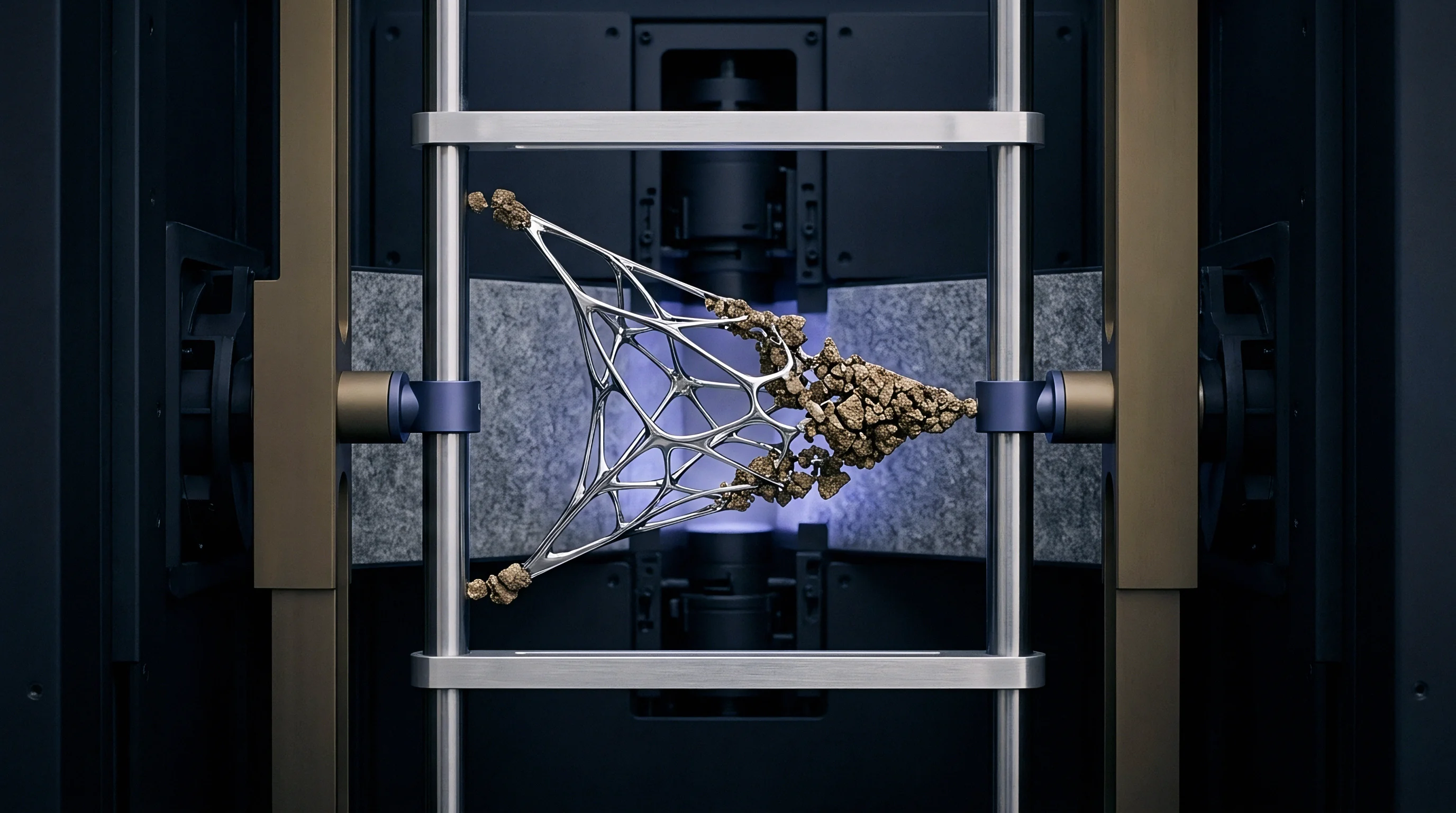
Electrode slitting defects directly govern downstream battery pack safety and manufacturing yield. Excessive slitting burrs along current collector edges puncture porous separator films during winding or stacking, causing localized internal micro-short circuits. Burrs exceeding 8.0 μm on cathode foils violate cell assembly tolerances, triggering automated cell rejection during end-of-line high-potential (hi-pot) dielectric testing.
Tooling wear directly increases burr height, making knife wear characterization a vital operational task for process engineering teams.
Establishing the physical relationship between carbide microstructure wear and burr growth kinetics involves continuous monitoring of edge profiles. The table below correlates tool wear states, characterized via BSE imaging, with observed burr dimensions on 12 μm aluminum cathode foils coated with high-nickel NMC active material.
| Slit Foil Cut Distance (m) | Tool Tip Radius via BSE (μm) | Dominant Carbide Degradation Mode | Mean Burr Height (μm) | Electrode Yield Factor (%) |
|---|---|---|---|---|
| 10,000 | 1.2 ± 0.2 | Initial polishing, no micro-fracture | 1.8 ± 0.4 | 99.6 ± 0.2 |
| 50,000 | 1.8 ± 0.3 | Cobalt loss along rake face | 3.1 ± 0.5 | 99.2 ± 0.3 |
| 100,000 | 2.6 ± 0.4 | Isolated grain pull-out | 4.8 ± 0.7 | 98.5 ± 0.4 |
| 180,000 | 3.9 ± 0.5 | Grain boundary micro-chipping | 7.6 ± 0.9 | 95.8 ± 0.6 |
| 250,000 | 5.8 ± 0.8 | Gross edge spalling and flank wear | 12.4 ± 1.8 | 88.2 ± 1.2 |
Calculating the landed cost impact of premature tool failure demonstrates the value of BSE-based tooling qualification. Assume a production line runs 200,000 meters of cathode coil per week across eight slitting stations. A low-grade carbide knife set costing 450 dollars exhibits grain pull-out at 80,000 meters, forcing two knife changeovers per week.
Each tooling change requires 90 minutes of line downtime, carrying an operational stoppage cost of 1,200 dollars per hour, alongside scrap generation of 150 meters of un-slit electrode during line re-threading. A qualified sub-micron carbide knife set costing 850 dollars lasts 200,000 meters before edge rounding induces burrs, eliminating mid-week changeovers.
The total weekly cost for the low-grade tooling includes 900 dollars in replacement blades, 3,600 dollars in downtime expenses, and 800 dollars in scrapped electrode material, totaling 5,300 dollars. The BSE-qualified tooling incurs 850 dollars in knife costs and zero mid-run downtime expenses, cutting operational slitting expenditure by over 4,400 dollars per station per week. Incorporating BSE tooling validation at incoming quality control preserves slitting line uptime and secures electrode yield targets.
Slitting quality settles the safety margin of the finished battery cell.

Protocol

Which Parameters Govern Tool Acceptance Audits?
Implementing a rigorous incoming qualification procedure for electrode slitting tooling requires codified quantitative metrics. Relying on vendor certificates of analysis leaves cell manufacturers vulnerable to sub-surface grinding damage, inhomogeneous cobalt distribution, and recycled carbide blending. A robust quality audit combines standardized physical sampling with automated backscattered electron microscopy routines.
The audit protocol selects three knives per manufacturing batch of fifty units, executing non-destructive inspection across four cardinal points on each circular blade. Technicians record high-resolution BSE image sets across five standard fields per point, evaluating binder dispersion, porosity volume fractions, and cutting tip radius values against clear pass-fail acceptance thresholds.
- Edge profile radius must measure below 1.8 μm across all cardinal quadrants under 10 kV BSE calibration.
- Cobalt binder depletion depth cannot exceed 0.25 μm from the ground flank face into the bulk tool matrix.
- Free carbon inclusion area must remain below 0.05% of the total cross-sectional area within a 50 μm boundary from the cutting edge.
- Transverse micro-crack count must equal zero across all analyzed high-resolution backscattered electron inspection frames.
Procurement agreements incorporate these BSE imaging metrics directly into binding tooling supply contracts. When incoming tooling lots fail the automated compositional thresholds, the supplier absorbs logistics expenses and replacement lead-time liabilities. Establishing these analytical criteria shifts verification from subjective dispute to objective physical measurement.
Process teams maintain strict inspection regimens to verify that cutting tools preserve edge sharpness across continuous high-volume production campaigns.