Intermetallic Compound Kinetics under Elevated Temperature Battery Operating Conditions
Elevated temperature battery operations accelerate interfacial intermetallic growth, requiring nickel diffusion barriers to prevent joint embrittlement.

Alloy
Dissimilar metal joining forms the backbone of lithium-ion cell tab interconnects and module busbar assemblies. Continuous operating temperatures between 45°C and 85°C supply the activation energy needed for solid-state atomic transport across these heterogeneous metallic boundaries. When aluminum cell tabs attach to copper busbars through ultrasonic wire bonding, laser welding, or resistance spot welding, the direct contact between two different crystal lattices initiates immediate interdiffusion.
The resulting solid-state reactions produce discrete intermetallic compound layers that alter the mechanical integrity and electrical conductivity of the junction over prolonged duty cycles.

Interface Phase Equilibrium in Dissimilar Welds
Direct thermal contact converts pure elemental boundaries into multi-phase metallurgical zones. In copper-to-aluminum joints, the local concentration gradient drives the phase transformation sequence dictated by the binary phase diagram. Heat drives diffusion.
Solid-state interdiffusion progresses through the localized formation of distinct phases including CuAl2 (thη phase), CuAl (η2 phase), and Cu9Al4 (γ2 phase). Each intermetallic phase possesses physical parameters markedly different from the base metals. CuAl2 forms preferentially at lower activation thresholds, whereas Cu9Al4 emerges under sustained elevated thermal conditions, introducing localized areas of high electrical resistivity and extreme brittleness.
Ultrasonic friction welding creates fine-grained non-equilibrium microstructures with high initial defect density. These microstructural defects act as fast-diffusion pathways during continuous storage or heavy discharge cycles at 60°C. Cold deformation stores energy. Consequently, elevated operating temperatures accelerate the transformation from metastable solid solutions into thermodynamically stable, highly stoichiometric intermetallic compounds.
The physical footprint of these interfacial zones expands over thousands of operational hours, consuming parent metal and compromising the electrical cross-section of the tab attachment.
- Theta phase formation occurs early at copper-aluminum boundaries, yielding a crystalline CuAl2 layer that doubles local electrical resistance.
- Gamma-two phase growth requires higher activation energy, developing adjacent to copper substrates under sustained 70°C exposure and inducing structural stiffness.
- Eta-two phase nucleation acts as an intermediate transition layer, exhibiting high thermodynamic stability and low fracture toughness.
- Solid solution saturation precedes intermetallic precipitation, establishing local lattice strains that lower the threshold for micro-crack initiation.

Solid State Diffusion Barriers and Coatings
Engineers apply metallic surface treatments to suppress direct interdiffusion between active busbar materials and terminal tabs. Electroplated nickel layers function as classic diffusion barriers due to the low diffusion coefficient of copper and aluminum within the nickel lattice at battery operating temperatures. Nickel barriers retard migration.
A electrodeposited nickel coating measuring 2.0 to 5.0 µm in thickness isolates copper substrates from aluminum tabs, shifting the thermodynamic reaction toward the slower Ni-Al intermetallic growth kinetics.
Alternative barrier systems include electroplated tin coatings, thin titanium adhesion layers, and chromium diffusion stops. Tin coatings facilitate lower-temperature soldering process flows but undergo rapid reaction with copper to yield Cu6Sn5 and Cu3Sn phase layers at temperatures as low as 50°C. Titanium barrier layers provide superior diffusion resistance up to 85°C, though high processing costs limit their deployment to specialized aviation or defense battery architectures.
| Intermetallic Phase | Crystal Structure | Electrical Resistivity (10⁻⁸ Ω·m) | Vickers Hardness (HV) | Formation Activation Energy (kJ/mol) |
|---|---|---|---|---|
| CuAl₂ (Theta) | Tetragonal | 8.0 | 410 | 78.5 |
| Cu₉Al₄ (Gamma-2) | Cubic | 14.2 | 580 | 112.0 |
| CuAl (Eta-2) | Monoclinic | 11.5 | 520 | 95.3 |
| Cu₆Sn₅ (Eta) | Monoclinic | 17.5 | 380 | 48.2 |
| Cu₃Sn (Epsilon) | Orthorhombic | 8.9 | 440 | 72.1 |
| NiAl₃ | Orthorhombic | 13.1 | 620 | 142.0 |
Vendors frequently attribute tab contact resistance growth to ambient moisture ingress rather than thermal phase evolution.

Growth
Solid-state interdiffusion kinetics at joint interfaces follow predictable thermodynamic laws modified by local strain and defect densities. Standard empirical models treat layer growth as a thermally activated diffusion process governed by Fickian migration across phase boundaries. Continuous duty cycles at elevated pack temperatures accelerate atomic exchange, causing sub-micron initial weld interfaces to expand into multi-micrometer thick brittle phase structures over time.
Arrhenius Kinetics of Bimetallic Systems
Mathematical modeling of phase boundary displacement relies on the Arrhenius relationship to capture temperature dependence. The rate constant K for intermetallic compound growth varies exponentially with absolute temperature according to the relation:
K = K0 expleft(-fracQR Tright)
Where K0 represents the pre-exponential frequency factor, Q is the effective activation energy for interdiffusion, R is the universal gas constant (8.314 J/mol·K), and T is the absolute junction temperature in Kelvin. Temperature governs reaction rates. Activation energy values dictate how sensitive a given joining technology is to thermal spikes.
For unplated copper-aluminum interfaces, effective activation energies range between 75 and 115 kJ/mol depending on joint deformation state. Nickel-plated interfaces exhibit significantly higher activation energies between 135 and 160 kJ/mol, creating a steep thermal barrier that halts atomic migration under standard automotive operating windows.
Parabolic Layer Thickening Mechanics
The total thickness x of an intermetallic layer growing under isothermal conditions evolves according to the parabolic rate law:
x = sqrtK · t = sqrtK0 expleft(-fracQR Tright) · t
Where t indicates continuous thermal exposure duration in seconds. Consider a comparative operational scenario evaluating bare copper-aluminum busbar lap joints against nickel-barrier busbar lap joints operating continuously at 65°C (338.15 K) inside a high-power commercial vehicle pack. Assume an initial non-equilibrium interfacial layer thickness of 0.10 µm post-laser welding.
For the bare Cu-Al interface, taking a pre-exponential factor K0 = 2.5 × 10⁻⁴ m2/s and an activation energy Q = 88.0 kJ/mol yields a parabolic growth constant:
KCu-Al = 2.5 × 10⁻⁴ · expleft(-frac880008.314 · 338.15right) = 2.5 × 10⁻⁴ · exp(-31.31) = 6.28 × 10⁻¹⁸ m2/s
Over a continuous exposure period of 3,000 hours (1.08 × 10⁷ seconds) at 65°C, the net intermetallic layer growth calculation demonstrates:
xCu-Al = sqrt6.28 × 10-18 m2/s · 1.08 × 10⁷ s = sqrt6.78 × 10-11 m2 = 8.23 × 10⁻⁶ m = 8.23 μm
Adding the initial weld layer yields a final interface thickness of 8.33 µm. Conversely, evaluating a nickel-barrier protected joint under identical conditions with K0 = 1.2 × 10⁻⁴ m2/s and Q = 145.0 kJ/mol produces:
KNi-barrier = 1.2 × 10⁻⁴ · expleft(-frac1450008.314 · 338.15right) = 1.2 × 10⁻⁴ · exp(-51.58) = 4.79 × 10⁻²⁷ m2/s
xNi-barrier = sqrt4.79 × 10-27 m2/s · 1.08 × 10⁷ s = 2.27 × 10⁻¹⁰ m = 0.00023 μm
The nickel electroplate effectively eliminates solid-state diffusion growth over the nominal operational lifetime of the battery module. Thicker layers degrade faster.
Continuous pack operation above fifty-five degrees Celsius doubles intermetallic growth rates for every seven degree increase.
- Precondition clean test coupons via solvent degreasing and micro-etching to ensure standardized initial surface energy across all bond pads.
- Execute high-precision laser lap welds utilizing standardized beam speed, focus position, and pulse profile parameters on specified terminal substrates.
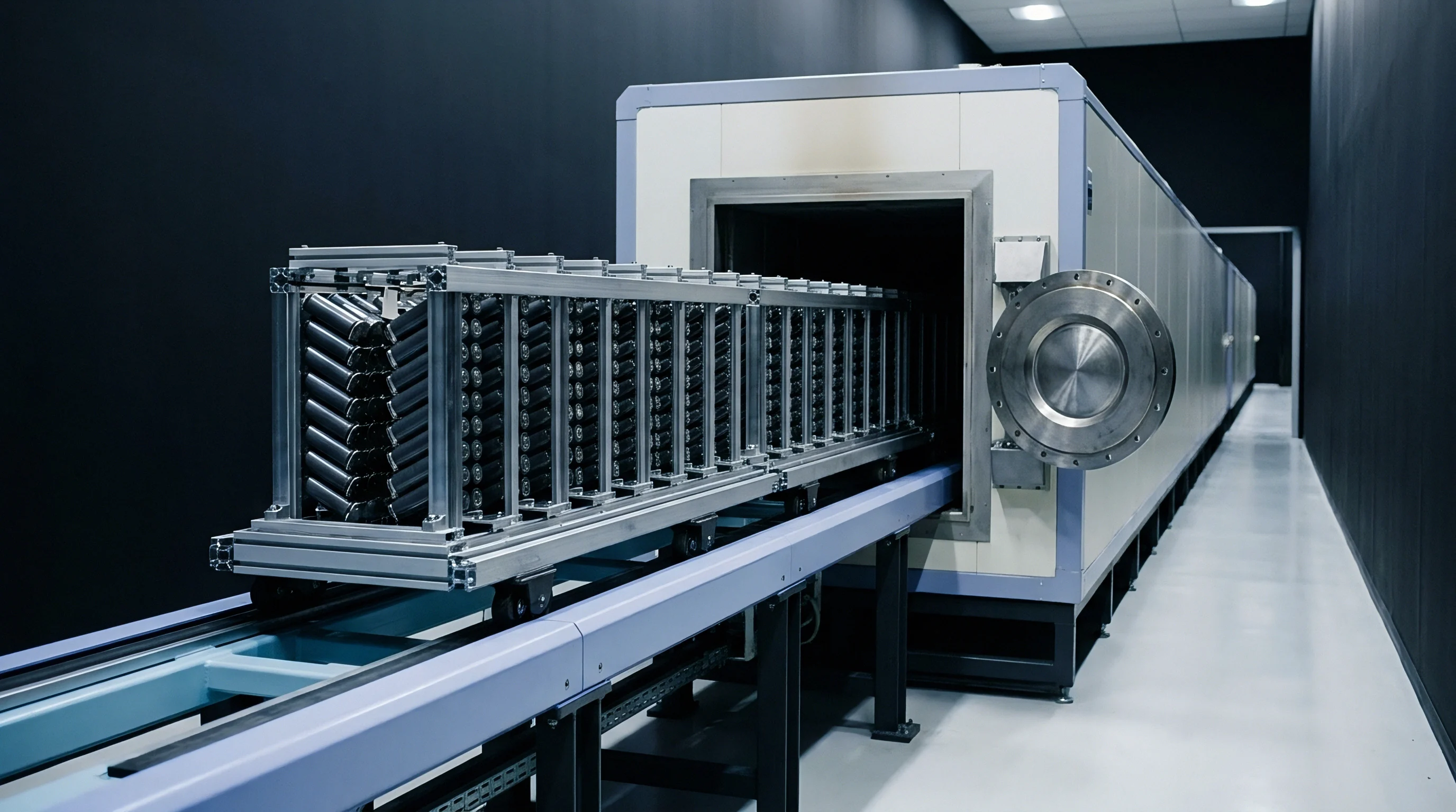
- Place test samples into environmental chamber environments set to isothermal conditions of 55°C, 70°C, and 85°C with controlled atmospheric purging.
- Extract sample batches at logged time intervals of 250, 500, 1000, 2000, and 3000 hours for non-destructive resistance characterization.
- Mount extracted joints in low-shrinkage cold-curing epoxy resin blocks to prevent mechanical disruption of fragile interfacial layers during sectioning.
- Perform high-resolution cross-sectional polishing and quantify layer growth progression utilizing field-emission scanning electron microscopy.
| Metallurgical System | Temperature (°C) | Parabolic Constant K (m²/s) | Layer Growth at 1,000 Hours (µm) | Layer Growth at 3,000 Hours (µm) |
|---|---|---|---|---|
| Bare Cu-Al (Ultrasonic Weld) | 45 | 4.12 × 10⁻¹⁹ | 1.22 | 2.11 |
| Bare Cu-Al (Ultrasonic Weld) | 65 | 6.28 × 10⁻¹⁸ | 4.75 | 8.23 |
| Bare Cu-Al (Ultrasonic Weld) | 85 | 6.85 × 10⁻¹⁷ | 15.70 | 27.19 |
| Bare Cu-Sn (Soldered Joint) | 55 | 1.84 × 10⁻¹⁷ | 8.14 | 14.10 |
| Bare Cu-Sn (Soldered Joint) | 75 | 1.42 × 10⁻¹⁶ | 22.60 | 39.14 |
| Ni Barrier / Cu-Al Interface | 65 | 4.79 × 10⁻²⁷ | 0.00013 | 0.00023 |
| Ni Barrier / Cu-Al Interface | 85 | 2.15 × 10⁻²⁴ | 0.00278 | 0.00482 |
Thinner diffusion layers maintain mechanical ductility whereas mature stoichiometric intermetallic phases yield brittle fracture under low-amplitude vibration.


Strain
Accumulation of intermetallic compounds introduces severe mechanical distortion across terminal interfaces. Mismatches in elastic modulus and thermal expansion parameters generate sustained localized stress fields during operational thermal cycling. Because intermetallic phase formation involves non-uniform volumetric transformation, severe lattice strain develops along the reaction front, destabilizing the mechanical bond between busbars and cell current collectors.
Kirkendall Void Nucleation under Thermal Cycling
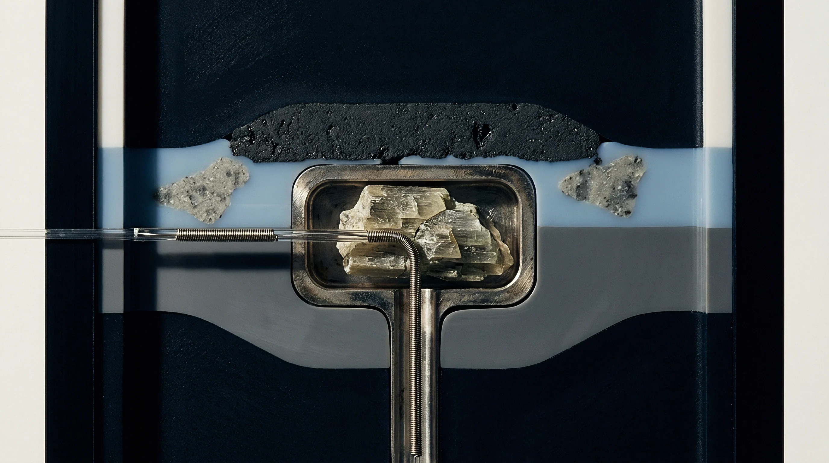
Differential atomic diffusion rates across dissimilar metal junctions induce vacancy flux imbalances. In copper-aluminum and copper-tin joints, copper atoms diffuse into the adjacent matrix significantly faster than aluminum or tin atoms diffuse backward into the copper lattice (DCu > DAl). Interfacial voids coalesce rapidly.
To compensate for this asymmetric atom flux, vacancies migrate in the opposite direction, super-saturating along the copper-intermetallic phase boundary.
Under continuous thermal cycles driven by fast-charging regimes, these microscopic vacancies nucleate into dense chains of Kirkendall voids. Void accumulation reduces the net load-bearing cross-sectional area of the weld pad, accelerating mechanical fatigue failure. Resistive losses rise nonlinearly.
As operational heat spikes recur, elevated stress concentrations frame each micro-void, creating ideal sites for crack initiation and rapid sub-critical crack propagation across the entire electrical interface.
Shear Yield Capacity and Fracture Modes
Intermetallic phase transformation fundamentally changes the mechanical performance of cell tab connections under shear and tensile loading. Base metals like copper and aluminum exhibit high ductility and extensive plastic deformation prior to failure. Conversely, compounds such as CuAl2 and Cu9Al4 feature high hardness values exceeding 400 HV combined with extremely low fracture toughness (KIc
Thermal expansion coefficient ($α) mismatches exacerbate mechanical cleavage. Pure copper possesses a CTE of approximately 16.5 × 10⁻⁶/K, pure aluminum exhibits 23.1 × 10⁻⁶/K, while the intermediate CuAl2 phase demonstrates 12.4 × 10⁻⁶/K. Cyclic thermal excursions generate high shear stresses along these brittle phase planes. When vibration loads from vehicle operation align with internal thermal strain fields, joint failure shifts from ductile parent-metal necking to brittle interfacial cleavage along the micro-voided intermetallic zone.
Compliance with UN 38.3 vibration testing requires pre-aged weld samples to demonstrate zero mechanical delamination after thermal conditioning.
Uncontrolled interfacial voiding reduces cross-sectional contact area, driving localized ohmic heating beyond thermal cutoff thresholds and causing localized pack failure.

Diagnosis
Detection of solid-state phase degradation requires high-resolution physical metrology paired with sensitive electrical diagnostics. Because intermetallic compound formation occurs within sub-micron zones buried beneath solid metal busbars, conventional visual or basic resistance measurements often fail to detect early-stage interface degradation. Comprehensive screening protocols integrate destructive metallurgical cross-sectioning with non-destructive frequency-domain impedance monitoring.
Cross Sectional Metallurgical Analysis
Precise characterization of interface microstructures relies on disciplined sample preparation protocols that preserve ultra-thin phase boundaries without introducing mechanical polishing artifacts. Mechanical failure follows cracking.
- Section the target joint using a slow-speed diamond wafering saw equipped with synthetic coolant to limit localized frictional heating during cutting.
- Encapsulate the sectioned joint in epoxy mounting compound engineered for zero shrinkage and high edge-retention characteristics.
- Grind the mounted specimen sequentially utilizing silicon carbide abrasive papers from 320 grit down to 1200 grit under ultra-pure water lubrication.
- Polish the surface using polycrystalline diamond suspensions down to 0.25 µm, followed by final colloidal silica polishing for 20 minutes.
- Etch the polished surface using dilute Keller’s reagent or ammonium persulfate solution to reveal grain boundaries and discrete intermetallic phases.
- Perform quantitative energy-dispersive X-ray spectroscopy line scans across the phase interface inside a field-emission electron microscope to verify phase stoichiometry.
How Does Intermetallic Layer Thickness Correlate with Contact Resistance?
Electrical resistance growth directly mirrors the physical consumption of high-conductivity base metals and the thickening of high-resistivity compound layers. Pure copper and aluminum possess room-temperature resistivities of 1.7 × 10⁻⁸ Ω·m and 2.7 × 10⁻⁸ Ω·m respectively. By contrast, intermetallic phases like Cu9Al4 exhibit resistivities reaching 14.2 × 10⁻⁸ Ω·m, representing an eight-fold increase in basic volume resistivity.
Thermal spikes accelerate degradation.
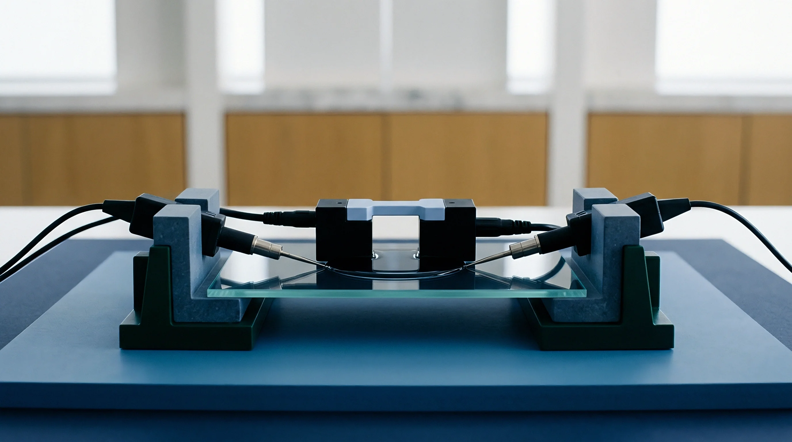
Four-point Kelvin resistance measurements capture sub-milliohm shifts across joint assemblies. High-frequency Electrochemical Impedance Spectroscopy (EIS) isolated between 1 kHz and 10 kHz detects subtle alterations in high-frequency real-axis intercept values (RΩ). As the intermetallic layer expands beyond a threshold thickness of 2.0 µm, local contact resistance rises nonlinearly.
Localized current crowding occurs at unvoided contact points, driving I2 R heat generation that further accelerates diffusion kinetics in a compounding thermal feedback loop.
Intermetallic thickness exceeding two micrometers increases interface electric resistance by more than three hundred percent at sixty-five degrees.
Whether in-situ high-frequency impedance monitoring can reliably distinguish between electrochemical cathode degradation and tab intermetallic growth during active field operation remains unproven.


Margin
Managing intermetallic degradation risks demands rigorous technical specification, explicit supplier compliance metrics, and clear contractual allocation of warranty liability. Failure to control interface kinetics during NPI phase design commits cell packs to unquantified field failures during late-stage warranty windows. Sourcing engineers mitigate these commercial exposures by mandating diffusion barrier standards directly within cell and pack supply contracts.
Specification Clauses for Interconnect Plating
Procurement documents must specify physical, chemical, and dimensional tolerances for all tab surface coatings. Relying on generic commercial plating notes invites wide quality variations between production lots. Standard specification clauses mandate minimum electrodeposited nickel thickness of 3.0 µm according to ASTM B568 x-ray fluorescence measurement protocols.
Diffusion barriers protect contacts.
Quality provisions must mandate zero pinhole porosity tested under ISO 10308 standards to eliminate microscopic reaction sites. Plating adhesion must survive 180-degree bend testing per ASTM B571 without micro-cracking or flaking. By establishing explicit First-Article Inspection metrics backed by automated batch sampling, pack integrators shift process drift liability back to cell and tab suppliers before committing tooling capital.
Warranty Reserves for High Temperature Cell Operation
Thermal degradation of interconnects directly impacts financial warranty allocations for packs deployed in hot ambient markets or heavy duty-cycle applications. Incorporating a 3.0 µm nickel barrier adds an estimated $0.04 to $0.12 in raw material and processing cost per cell terminal. Contact failure halts current.
Conversely, omitting diffusion protection increases field failure rates by up to 3.5% over a 10-year design life operating at elevated average ambient temperatures.
| Interface Architecture | Added NRE / Tooling Cost per Pack | Unit Cost Impact per Cell Tab | Expected Life at 65°C Continuous (Hours) | Projected Field Failure Rate at Year 8 (%) |
|---|---|---|---|---|
| Direct Cu-Al Laser Weld (No Barrier) | $0 | $0.00 | 1,800 | 4.20 |
| Bare Cu-Sn Soldered Interconnect | $0 | +$0.02 | 850 | 8.50 |
| Electroplated Ni Barrier (3.0 µm) | $12,000 | +$0.06 | 20,000 | 0.05 |
| Clad Ni-Al Composite Tab Structure | $35,000 | +$0.18 | 25,000 | 0.01 |
| PVD Titanium Adhesion Layer + Ni | $85,000 | +$0.45 | 30,000 | 0.001 |
Phase transitions absorb strain. Quantifying the landed cost of quality requires balancing front-end plating NRE against back-end reserve provisions. High-temperature qualification trials must validate that interfacial resistance growth remains under 10% across 3,000 hours of continuous 65°C aging before releasing production volumes.
Plating defects beneath three micrometers allow accelerated solid state diffusion across terminal interfaces.
Inserting a mandatory maximum interfacial resistance cap of fifty micro-ohms after five hundred hours at sixty-five degrees Celsius into purchase contracts transfers premature tab joint failure liability back to the supplier.