Resolving Non-Destructive Inline Metrology Limitations for Sub-Surface Electroplating Interfacial Micro-Void Identification
Resolve inline electroplating void detection limits by coupling multi-frequency eddy current screening with automated diversion to phase-contrast X-ray computed tomography.

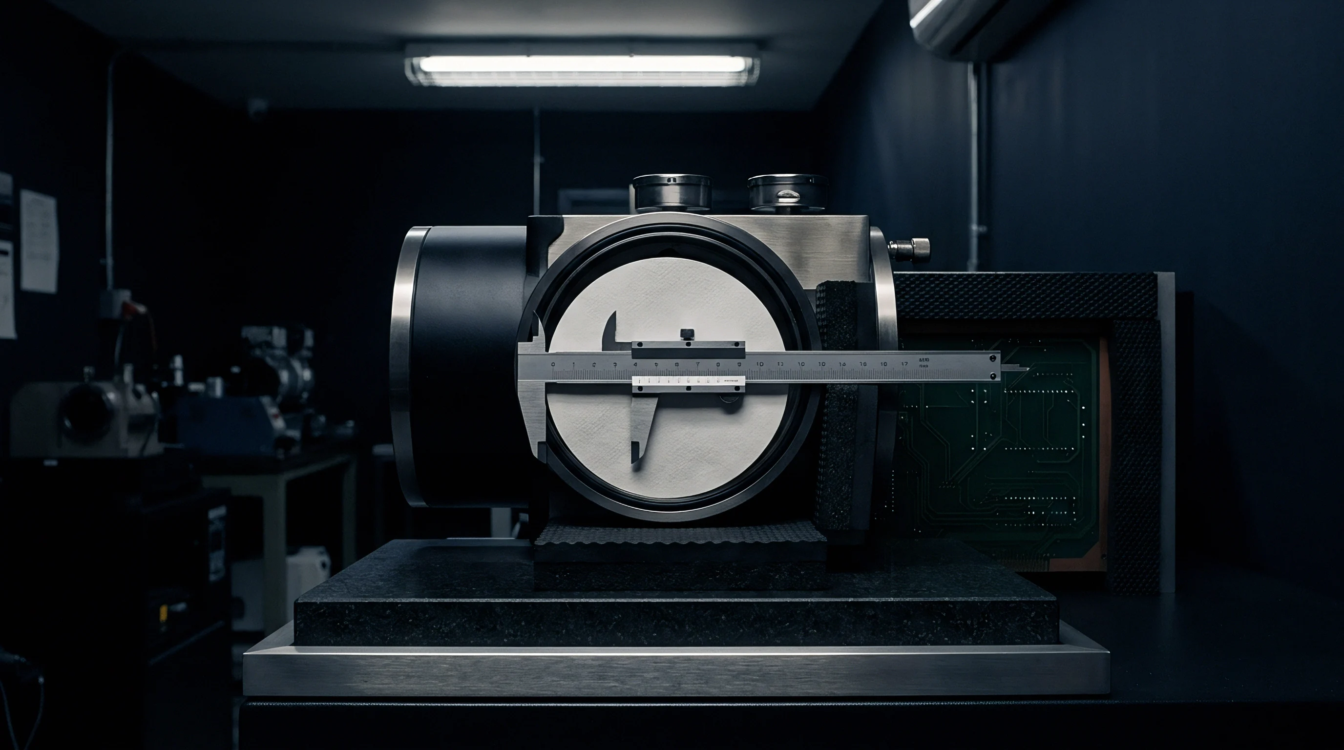
Foil
Electroplated copper foil substrates and nickel-plated busbar tabs present sub-surface interfacial cavities that escape standard optical line cameras. At line speeds exceeding 40 meters per minute for current collector rolls or 60 parts per minute for tab welding fixtures, sub-micron voids remain hidden beneath dense electrodeposited metal skins. A raw thickness variation of ±0.3 micrometers in a 6-micrometer copper foil masks localized plating delaminations where bath brighteners or hydrogen gas pockets prevent planar metallurgical bonding.
When these current collectors enter slurry coating and calendering, unbonded regions rupture under roll compaction pressures exceeding 150 megapascals, producing active material shedding and pinhole short circuits.
Tab-to-busbar joints show identical physical failure sequences. Prismatic cell caps use copper or aluminum base terminals electroplated with 3 to 8 micrometers of nickel to prevent galvanic oxidation and assist ultrasonic or laser joining. Micro-voids concentrating at the substrate-plating interface reduce the contact area, raising localized electrical interfacial resistance by 15 to 45 micro-ohms per joint.
Under continuous pack discharge rates of 3C to 5C, this localized impedance generates hotspots reaching temperatures above 90 degrees Celsius, accelerating solid electrolyte interphase degradation in adjacent pouch seals.
A raw contact resistance elevation of 20 micro-ohms across an electroplated terminal post increases joint operating heat generation by four watts during continuous 200-ampere discharge.
Metrology systems deployed inline face fundamental physics trade-offs between acquisition speed and spatial resolving power. Standard factory lines rely on beta backscatter gages and continuous eddy current lift-off sensors. These tools measure bulk mass per unit area or average electrical conductivity over sensor spot sizes between 5 and 15 millimeters.
A sub-surface micro-void measuring 0.5 to 3.0 micrometers in lateral diameter creates an impedance disturbance four orders of magnitude smaller than the baseline noise floor of an inline eddy current sensor moving over a vibrating web.
Suppliers routinely dismiss these baseline micro-cavities as benign wetting variations that settle permanently once laser welding melts the bulk plating stack.
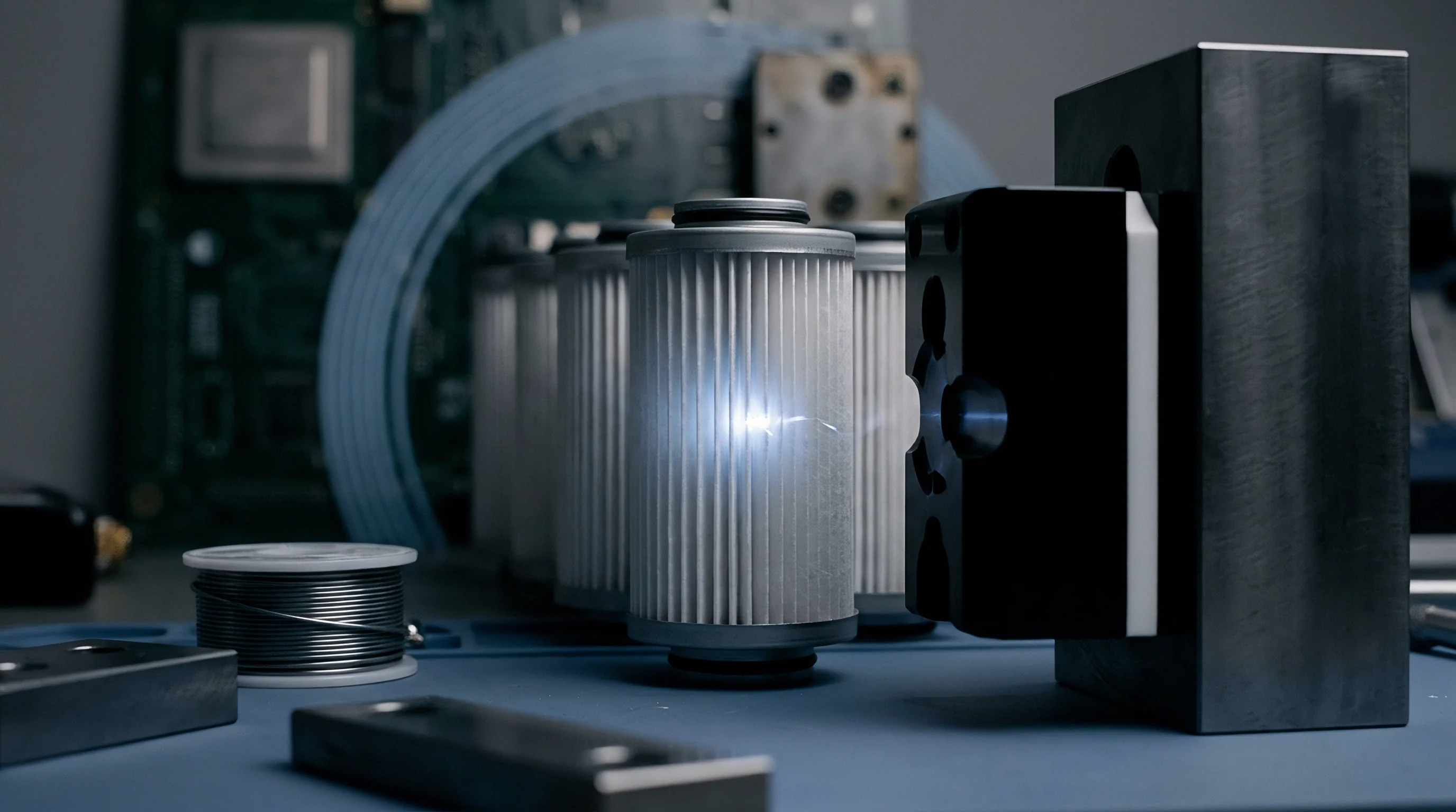

Frequency
Electromagnetic penetration depth dictates the physical boundary of high-frequency inline eddy current inspection. The skin depth equation couples excitation frequency, electrical conductivity, and magnetic permeability into a finite detection window. In pure electroplated copper with an International Annealed Copper Standard conductivity of 100 percent (5.80 × 10⁷ Siemens per meter), an excitation frequency of 1 megahertz limits the standard penetration depth to 66 micrometers.
Pushing excitation frequencies upward to 10 megahertz compresses the skin depth to 21 micrometers, concentrating electromagnetic fields near the electroplate-to-substrate boundary.

Can High-Frequency Eddy Current Resolve Subsurface Cavities?
Signal-to-noise ratios degrade severely as the excitation frequency crosses the 5 megahertz threshold in production environments. Lift-off variations between the sensor face and the travelling strip introduce phase shifts that mimic changes in substrate density. A physical displacement of 2 micrometers caused by roller runout creates an apparent resistance variation equivalent to a 50-micrometer interfacial separation.
Phase angle discrimination separates lift-off noise from true sub-surface density losses. Operating multi-channel array probes with differential coil configurations yields orthogonal vector components where the resistive axis tracks metal thickness and the reactive axis isolates boundary defects. Differential sensors cancel common-mode thermal drift and web flutter.
Micro-voids concentrate localized current density. When the defect diameter drops below 10 percent of the coil diameter, the electromagnetic field shunts around the defect without producing measurable flux linkage changes.
| Metrology Modality | Effective Lateral Resolution | Depth Penetration Range | Measurement Cadence | Primary Detection Mechanism | Industrial Bottleneck |
|---|---|---|---|---|---|
| Multi-Frequency Eddy Current | 20 to 50 micrometers | 10 to 80 micrometers | 100 kHz sample rate | Perturbation of induced eddy current vector fields | Lift-off sensitivity from web mechanical vibration |
| Laser Ultrasonic Acoustics | 2 to 5 micrometers | 1 to 500 micrometers | 500 Hz point pulse | Acoustic impedance mismatch reflection at void wall | Photothermal ablation risks on thin foil substrates |
| Line-Scan TDI Radiography | 1 to 3 micrometers | Full thickness penetration | 15 meters per minute | Differential X-ray photon absorption across density steps | Takt mismatch requiring offline statistical diversion |
| Laser Flash Thermography | 15 to 30 micrometers | 5 to 40 micrometers | 20 Hz frame rate | Transient thermal boundary resistance accumulation | Surface emissivity variations across raw plating baths |
Evaluating an incoming batch of electroplated copper foils requires mapping defect populations against acoustic and electromagnetic responses. Voids originate from distinct electrochemical mechanisms during high-speed bath deposition:
- Hydrogen inclusion pockets form when cathode current efficiencies drop below 95 percent during sudden current density spikes.
- Organic additive entrapment occurs when brightener molecules fail to desorb before subsequent metal monolayers deposit over the growth front.
- Substrate oxide micro-blisters generate incomplete metallurgical wet-out over underlying raw metal rolled strip seams.
- Kirkendall micro-void clusters evolve along the intermetallic boundary when plated nickel layers experience subsequent thermal drying cycles above 180 degrees Celsius.
Laser-generated surface acoustic waves provide an alternative approach by combining optical excitation with interferometric detection. A pulsed nanosecond laser induces thermoelastic expansion on the plated surface, launching high-frequency Rayleigh waves whose energy concentrates within one acoustic wavelength of the boundary. At acoustic frequencies of 200 megahertz, Rayleigh wavelengths in copper measure approximately 11 micrometers.
When these waves encounter a sub-surface void, wave scattering and velocity dispersion alter the transient arrival waveform detected by a balanced photorefractive interferometer. Acoustic attenuation rises at gigahertz frequencies.
Acoustic reflection at a metal-to-void interface approaches total reflection because gas cavities provide near-zero acoustic impedance.
Higher excitation frequencies isolate shallow interfacial boundaries while lower frequencies pass through defects undetected.

Scatter
Photon attenuation models govern transmission radiography when inspecting electroplated terminal posts and cylindrical cell header discs. X-ray absorption follows the Beer-Lambert law, where the transmitted photon intensity decays exponentially as a function of the material mass attenuation coefficient, material density, and path length. Nickel exhibits a mass density of 8.90 grams per cubic centimeter, while copper measures 8.96 grams per cubic centimeter.
The minute radiographic contrast between these adjacent transition metals prevents simple threshold segmentation from identifying interfacial gaps.
When an interfacial micro-void measuring 1 micrometer in thickness sits beneath 5 micrometers of nickel plating and 500 micrometers of copper substrate, the total optical path length reduction represents less than 0.2 percent of the overall attenuation path. Standard flat-panel detectors with 16-bit analog-to-digital converters cannot separate this fractional transmission increase from the Poisson noise intrinsic to high-flux X-ray tube outputs. X-ray line sensors saturate quickly.
Phase-contrast imaging addresses this limitation by recording the spatial phase shift of coherent X-ray wavefronts refracted at void edges rather than relying on pure amplitude attenuation.
Refraction angles across a micro-void boundary scale inversely with photon energy and directly with electron density gradients. At an operating acceleration voltage of 90 kilovolts with a microfocus source spot size of 2 micrometers, phase refraction creates edge-enhancement fringes that amplify void boundary visibility by a factor of 8 relative to absorption contrast alone. Talbot-Lau grating interferometry implements this phase sensitivity without requiring synchrotron coherence sources.
Three transmission gratings placed between the source and detector split, shear, and recombine the beam, transforming sub-micron interfacial phase distortions into intensity fringes observable on standard industrial flat panels.
Standard ISO 1027 establishes radiographic image quality class B requirements where wire penetrameters must resolve thickness variations below one percent of total nominal wall dimension.
Industrial deployment faces geometric magnification penalties. Achieving a 1-micrometer voxel resolution on a pack busbar joint requires placing the specimen within 5 millimeters of the X-ray tube focal spot while positioning the detector 500 millimeters downstream. This 100-times magnification limits the instantaneous field of view to 2 square millimeters.
Inspecting a continuous strip or a high-takt battery cell terminal line requires stitching millions of frames, introducing computational overhead that forces lines to downsample data or divert cells into offline quarantine buffers.
Thermal reflection reveals buried delamination. In photothermal radiometry, an intensity-modulated laser beam excites thermal waves that diffuse downward through the electroplated layer. When these planar thermal waves encounter a sub-surface micro-cavity, the zero thermal conductivity of the entrapped gas acts as an insulating barrier, reflecting thermal energy back to the surface.
A high-speed mid-wave infrared camera records the surface temperature phase shift relative to the laser excitation pulse. Phase angles shift under voiding.
Thermal diffusivity in copper reaches 1.11 × 10⁻⁴ square meters per second, demanding infrared frame rates above 1000 frames per second to resolve thermal reflections returning from depth layers shallower than 10 micrometers. Surface roughness variations and plating bath gloss fluctuations alter optical emissivity, corrupting phase measurements unless radiometric data undergoes two-color normalization against reference blackbody calibrations.
The metrology community has not determined whether inline phase-contrast interferometry can distinguish between harmless closed micropores and planar sub-surface disbond networks across fluctuating web tensions without slowing line speeds below profitable production thresholds.

Takt
Factory line timing imposes non-negotiable boundaries on non-destructive metrology architectures. A modern pouch cell production line operates at 40 to 60 parts per minute, providing a cycle budget of 1.0 to 1.5 seconds per cell. During this measurement window, an automated inspection station must mechanically position the cell, acquire sensor data across four to eight separate terminal interfaces, process gigabytes of raw telemetry, execute feature classification algorithms, and trigger a diverter gate.
Nickel layers mask sub-surface density drops.

Is Acoustic Wavefront Tracking Feasible under Production Demands?
Scanning acoustic microscopy produces the highest spatial fidelity for interfacial micro-voids, resolving disbond areas smaller than 2 micrometers using 200 megahertz transducers. Acoustic wave propagation requires a physical coupling medium, typically deionized water or specialized fluoropolymer delay lines. Submerging dry battery terminals or unsealed pouch cells into liquid couplants contaminates electrolyte-sensitive chemistries, forcing manufacturers to deploy dry-contact elastomer rollers or non-contact air-coupled transducers.
Air-coupled acoustics suffer immense impedance mismatches. The acoustic impedance of air measures 413 Pascal-seconds per cubic meter, whereas copper measures 41.8 × 10⁶ Pascal-seconds per cubic meter. This interface reflects 99.999 percent of incident acoustic energy, leaving an infinitesimal signal fraction to enter the metal and interrogate the sub-surface plating boundary.
High-power piezoelectric transmitters driving focused transducers overcome transmission losses, but signal attenuation in ambient air caps the practical excitation frequency at 2 megahertz. At 2 megahertz, acoustic wavelengths in copper measure 2.3 millimeters, making the detection of a 2-micrometer interfacial void physically impossible through air-coupled acoustics.
| Inspection Strategy | Takt Time Per Joint | Void Cutoff Threshold | False Positive Rejection Rate | False Negative Escape Rate | Capital Expense Per Workcell |
|---|---|---|---|---|---|
| Full Inline Multi-Point Eddy Current Array | 0.8 seconds | 25 micrometers | 1.2 percent | 4.5 percent | 180,000 USD |
| High-Speed Laser Flash Thermography | 1.2 seconds | 15 micrometers | 2.8 percent | 1.8 percent | 240,000 USD |
| Offline Statistical Computed Tomography (2 Percent Sample) | 180 seconds | 0.8 micrometers | 0.1 percent | 0.01 percent | 850,000 USD |
| Hybrid Inline Dual-Modality Optical Eddy Station | 1.1 seconds | 8 micrometers | 0.9 percent | 0.4 percent | 390,000 USD |
Resolving this takt mismatch requires a split-architecture metrology model. The manufacturing line deploys high-speed screening tools executing statistical process control, coupled with automated divert gates that direct flagged cells into a secondary computed tomography cell. The secondary inspection cell operates at lower speeds with higher spatial sensitivity, confirming whether flagged anomalies represent fatal interfacial voids or harmless surface wrinkles.
Engineering teams qualify this screening sequence through rigorous multi-step inspection workflows:
- Differential sensor zeroing eliminates background thermal drift across conveyor fixtures by referencing an unplated substrate standard every fifty cycles.
- High-speed optical triangulation captures surface topography profiles with 0.1-micrometer vertical accuracy, isolating physical geometric variations prior to electromagnetic testing.
- Dynamic multi-frequency excitation sweeps frequencies between 500 kilohertz and 8 megahertz, extracting real-time impedance locus trajectories across the electroplated zone.
- Autonomous threshold classification correlates localized impedance dips against calibrated reject boundaries established during initial tool pilot builds.
- Statistical lot divergence automatically isolates the preceding and succeeding twenty cells whenever three consecutive packs exhibit anomalous phase deviations exceeding three standard deviations.
Cell internal resistance jumps measurably. When an inline metrology system fails to catch sub-surface electroplating voids, defective joints enter ultrasonic tab welders where localized acoustic coupling fails unpredictably. The unbonded electroplate tears away from the substrate copper, producing intermittent open circuits, elevated joint temperatures, and catastrophic field recalls that eliminate pack profit margins.

Seam
Commercial contracts and quality assurance dossiers define where operational accountability falls when latent plating defects escape inline factory detection. Cell buyers ordering prismatic or cylindrical units historically inspect only incoming external mechanical dimensions and open-circuit voltages. Internal electroplating integrity on foil current collectors or internal tab seams remains invisible to standard warehouse receiving protocols.
Pack warranty liabilities transfer upstream.
Lithium-ion cells operating under heavy industrial duty cycles experience cyclical mechanical expansion. An electroplated current collector carrying sub-surface micro-voids undergoes cyclic shear strains between active material coatings and the metal foil. Over 1000 charging cycles, these micro-voids coalesce into continuous interfacial delamination cracks.
Active material separates from the current collector, causing capacity retention to drop below the 80 percent warranty baseline long before the rated cycle life target.
Automotive qualification frameworks under USABC and IEC 62660 require suppliers to prove interface survivability under severe mechanical shock and thermal cycling. Sourcing contracts must explicitly define acceptable defect area fractions within electroplated boundaries rather than relying on ambiguous commercial trade terms. Tab pull strength drops sharply.
A contract line specifying IPC-4562 Grade 3 copper foil limits allowable sub-surface pinholes and interfacial porosity to zero detectable occurrences across a three-square-meter sample strip evaluated by scanning electron microscopy.
Factory audits must examine plating line chemistry logs alongside metrology calibration certificates. Plating tank organic additive concentrations, cathode current density curves, and continuous filtration turnover rates directly govern whether interfacial micro-cavities form during deposition. When an electroplating vendor operates baths near chemical depletion limits, the incidence of sub-surface micro-porosity spikes tenfold, defeating inline inspection setups calibrated against clean master standards.
Section 7.3 of automotive supply agreements establishes that latent interfacial defects traceable to upstream electroplating process instability invalidate standard 12-month defect reporting limitations, transferring all warranty recall expenditures directly to the cell manufacturing tier.