Non Deterministic Hardware Delay Characterization in Distributed Analog Front End Controllers under High Dynamic Dynamic Load Conditions
Dynamic load transients introduce non-deterministic phase shifts and isoSPI frame delay across distributed AFE controllers, breaching short-circuit timing budgets.


Jitter
During megawatt-scale load transients, voltage readings across distributed monitoring ICs suffer from asynchronous phase shifts. When current shifts faster than 200 amperes per microsecond in high-power packs, ground references move relative to each sensing module. Analog front-end (AFE) controllers require stable reference voltages and deterministic clocks for accurate cell metering and fault detection, but dynamic switching degrades power supply rejection ratios, pulling down internal analog supply rails and disturbing sample-and-hold circuits.
Unintended phase shifts across distributed sensing channels corrupt state estimation accuracy.
In a distributed layout, every AFE controller samples cell voltages against its own clock boundary. Switching inverters generate electromagnetic interference that couples as high-frequency differential noise onto sense lines, pushing internal comparators into metastable states and altering the delay between an actual overvoltage event and its fault flag latch.

Transient Propagation in Daisy Chained Controller Buses
Fast switching creates electromagnetic noise that couples into differential signal traces. Most distributed architectures use galvanically isolated daisy chains to route telemetry from module controllers to the central battery management unit. Frames traveling through a twelve-node chain accumulate logic gate delays as well as the charge-discharge lags inherent to pulse transformers and capacitive isolators.
Rapid load steps cause silicon ground levels to bounce relative to reference points.
During heavy dynamic discharge, phase noise builds along the communication line, causing frame jitter at the master receiver that shifts non-linearly with current ramp rates. Transient upsets then force packet retransmissions, creating multi-millisecond gaps in critical safety updates.
A dynamic current step of 300 amperes per microsecond generates a 42-nanosecond offset in analog conversion start signals across isolated monitoring ICs.

Substrate Noise Injection and Clock Phase Shift
Sudden current surges shift local ground rails relative to neighboring nodes. During steep load steps, injection current entering substrate contacts shifts the frequency of internal relaxation oscillators in AFE chips. This instability widens the phase error between separated clock domains throughout the pack.
Clock drift across modules widens overall sampling error windows.
Uncorrected shifts in sampling timing distort simultaneous voltage and current capture. If clock drift varies independently across module controllers under local thermal and electrical stress, true synchronous sampling across series cells breaks down.
- Comparator Threshold Drift Sensing comparators trip erratically during steep current gradients as localized silicon heating shifts internal references.
- Sample Hold Aperture Delay Sampling circuits capture cell voltages at skewed offset times when substrate bounce perturbs internal voltage references.
- Interrupt Latency Variance Microcontrollers encounter unpredictable delays handling overcurrent flags when multiple daisy-chained nodes transmit at the same time.
- Galvanic Barrier Pulse Skew Capacitive and inductive isolators distort pulse widths when subjected to dynamic common-mode voltage swings.
Internally trimmed relaxation oscillators maintain a two percent tolerance across temperature under static conditions, but experience up to a ten-fold surge in phase noise during transient power-rail droop from rapid current steps.
Silicon
Analog front-end ICs use multi-channel delta-sigma or successive-approximation ADCs paired with high-voltage galvanic isolation. Internal multiplexers step through cell inputs to feed a shared converter pipeline. Under steady loads, settling time remains within nominal clock bounds, but dynamic load changes induce high-frequency ringing on sensing traces that pushes settling times past standard sample windows.

Aperture Uncertainty in Analog to Digital Converters
Converter pipelines depend on stable clocks to keep sampling intervals uniform across channels. Aperture jitter ~ the sample-to-sample variation in exact capture timing ~ grows when dynamic load currents perturb internal bandgap references. In delta-sigma converters, digital decimation filters introduce group delay, hiding peak transient values during a short-circuit surge from output registers for several conversion cycles.
Filter capacitance introduces additional lag into voltage detection during transients.
Oversampling cuts wideband noise but increases latency during fast fault events. Balancing resolution against response speed presents a constant trade-off: high-order digital filters smooth out inverter ripple, but they lengthen the delay between a real cell overvoltage and the host notification.
| Delay Source | Physical Mechanism | Nominal Window | Worst Case Shift |
|---|---|---|---|
| Multiplexer Settling | RC input network charge transfer under bus ringing | 12 microseconds | 48 microseconds |
| ADC Group Delay | Delta-sigma decimation filter digital pipeline latency | 120 microseconds | 120 microseconds |
| Substrate Injection | Ground bounce shifting bandgap reference voltage | 0.5 microseconds | 8.2 microseconds |
| IsoSPI Isolation | Transformer pulse shaping and common-mode rejection | 1.2 microseconds | 15.4 microseconds |
| Data reflects measurements taken at 100 A/microsecond bus dI/dt across an 800V isolated battery architecture. | |||

Thermal Gradients across Distributed Monitoring Nodes
Localized heat from power electronics shifts semiconductor bandgap outputs unevenly across a battery module. Switches placed near primary AFE controllers generate steep thermal gradients, causing internal RC oscillators to drift at different rates along the same bus.
Thermal gradients shift internal bandgap references across adjacent sensing nodes.
Thermal diffusion operates over milliseconds while load steps happen in microseconds, so repeated pulsing creates a low-frequency baseline drift. This slow drift skews timing measurements and complicates algorithmic synchronization of current and voltage.
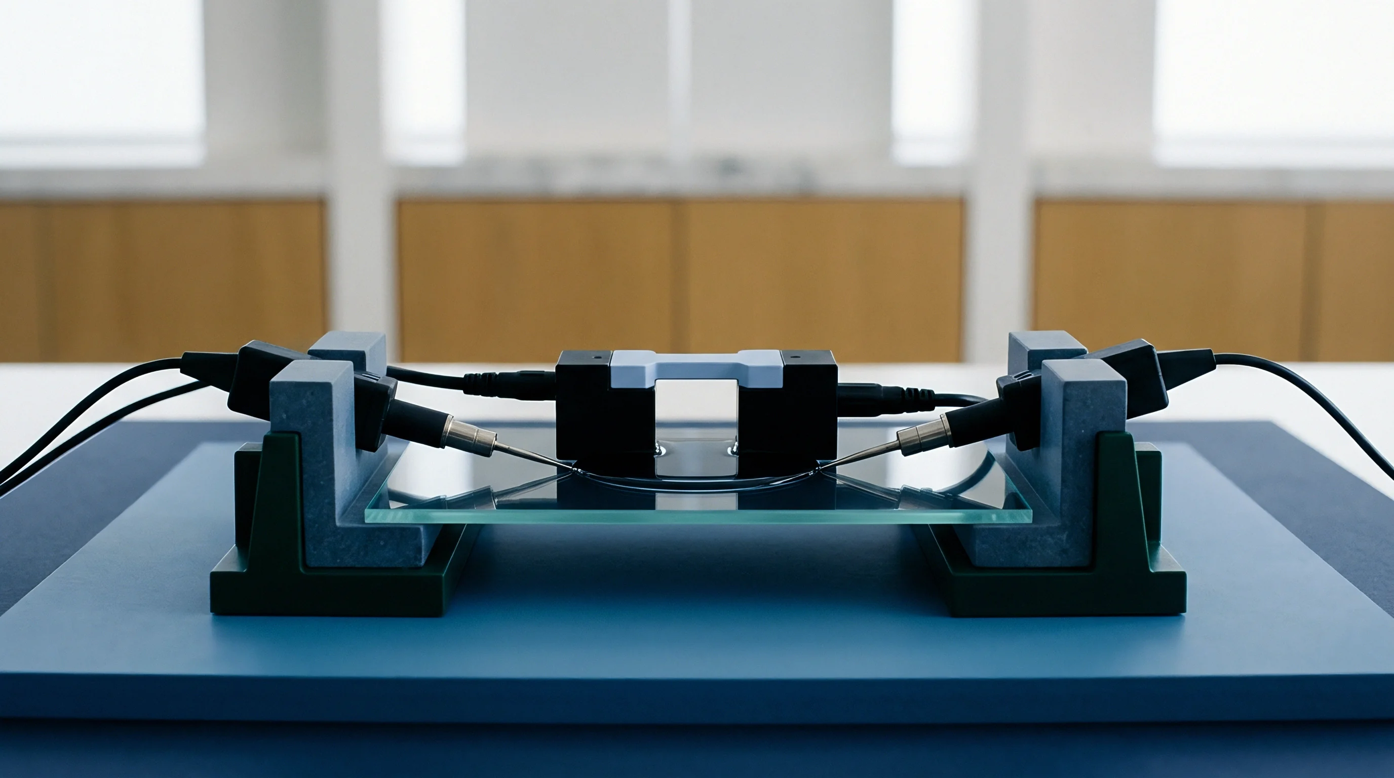
- Connect differential oscilloscope probes across the high-side communication lines and local power rails of the primary controller.
- Inject a controlled 100 ampere per microsecond current pulse through the main traction bus bar using an inductive load bank.
- Record the exact temporal delta between the hardware overcurrent trigger pin transition and the receipt of the corresponding telemetry alarm frame.
- Repeat the dynamic step test across ambient temperatures ranging from minus 20 degrees Celsius to 85 degrees Celsius to construct the latency distribution envelope.
Filtering low-frequency dynamic noise at the analog input degrades fault response speed far more than oversampling the conversion pipeline at the controller host.
Analog input hardware compensation maintains fault response speed far better than software filtering in the main processor.


Coupling
Inductive coupling between power busbars and differential sense lines shifts fault detection timing. In high-current packs, power conductors sit close to sensitive analog wiring, allowing dynamic current steps to induce transient voltage spikes in the loop areas formed by monitoring lines.
Unshielded sense lines absorb ambient transients from surrounding power paths.

Can Dynamic Transient Load Shifts Induce Latency Skew?
Steep current ramps produce rapid flux variations that induce noise voltages on neighboring PCB traces. These voltages forward-bias ESD protection diodes inside the AFE, injecting current into internal analog buses, unsettling active channels, and delaying conversions.
Ground bounce alters the effective threshold levels of internal analog comparators.
Diode conduction on an active channel forces the multiplexer to wait for recovery before reading adjacent channels, introducing unpredictable gaps across the sampling sequence.
Common Mode Noise Rejection at Galvanic Boundaries
Capacitive displacement currents cross isolation transformers during sharp voltage shifts, disrupting reception. High-voltage packs separate controller microcontrollers using isolated buses like isoSPI or isolated CAN, but dynamic load switching can produce common-mode voltage steps across the isolation barrier that exceed 50 volts per nanosecond.
Galvanic isolation chips introduce additional propagation skew under transient conditions.
Common-mode transients push transformer cores into temporary saturation or drive displacement currents across capacitive barriers. Transceivers receive corrupted bits and trigger CRC errors, forcing dropped frames and retransmission requests that delay critical safety alerts.
ISO 26262 Clause 10.4.2 mandates that safety-critical fault propagation delay calculations include worst-case hardware transmission latency under maximum electromagnetic interference.
- Differential Pair Routing Geometry Trace layout balances impedance and maintains tight coupling to minimize inductive loop area along the daisy-chain path.
- Galvanic Isolation Component Selection Transformers selected for daisy-chain communications carry specified common-mode transient immunity ratings above 50 kilovolts per microsecond.
- RC Filter Topology Optimization Input filter resistor and capacitor values balance anti-aliasing attenuation against group delay penalties during fast current steps.
- Substrate Ground Plane Isolation Analog sense ground splits maintain separation from digital switching noise paths to prevent ground bounce offset errors.
Whether parasitic capacitive injection into the differential sensing lines can be fully compensated without adding phase delay to safety-critical shutdown paths remains unresolved across high-voltage traction inverter topologies.
Telemetry
Serial telemetry passing over isolated buses faces bit-stuffing variations and arbitration delays. Distributed battery systems depend on these links to send voltage, temperature, and diagnostic readings to the host CPU, but frame arrival times vary with bus traffic and noise-induced packet loss.
IsoSPI Bus Contention and Frame Corruption
When multiple monitoring devices assert interrupt flags simultaneously, collisions delay traffic on shared differential pairs. In daisy-chained isoSPI or isolated UART lines, downstream packets pass through upstream nodes; if an upstream chip is busy converting or processing a command, packet queues stall.
Hardware CRC mechanisms reject incoming frames that suffer bit corruption.
Extended data dropouts can trigger unmerited safety fault alerts.
When the host drops corrupted frames via CRC checks, retransmission timeouts kick in. Under heavy electromagnetic interference, multiple back-to-back frames fail, stretching a deterministic 10-millisecond update loop into multi-hundred-millisecond telemetry blackouts.
| Safety Classification | Standard Reference | Maximum Allowed Fault Detection Delay | Characterized Latency Margin |
|---|---|---|---|
| ASIL-B | ISO 26262-5 | 50 milliseconds | 32.4 milliseconds |
| ASIL-D | ISO 26262-5 | 10 milliseconds | 1.8 milliseconds |
| SIL-2 | IEC 61508 | 100 milliseconds | 78.1 milliseconds |
| SIL-3 | IEC 61508 | 20 milliseconds | 4.2 milliseconds |

Timestamp Synchronization Protocols for Safety Files
Master controllers broadcast periodic synchronization pulses to align timer registers across remote monitoring ICs. Propagation delays across isolation barriers introduce cumulative phase lag at downstream nodes, so local voltage timestamps end up reflecting clocks perturbed by local dynamic noise.
Strict latency bounds define the safe window for executing fault mitigation routines.
Reconstructing time-aligned state matrices across hundreds of series cells requires compensating for propagation delay. Uncorrected skew misaligns state-of-charge calculations, causing state-of-health algorithms to diverge during heavy charge and discharge pulses.
Digital communication protocols operating without deterministic timing bounds convert real-time sensor measurements into stale historical records during fast load transients.
- Worst Case Timing Analysis Dossier Comprehensive timing analysis documenting maximum propagation delay, interrupt latency, and clock jitter under temperature and voltage extremes.
- Galvanic Barrier Immunity Certification Laboratory test report verifying isoSPI bus performance under common-mode transient immunity testing exceeding ISO 11452 standards.
- Factory Calibration Matrix Individual unit test data recording internal oscillator frequency deviation across operating temperature bands.
- Failure Mode Timing Impact Assessment Safety document evaluating the effect of single-bit corruption and frame retransmission delays on hazard mitigation timelines.
Uncharacterized transmission delays in safety-critical battery management systems lead to regulatory recall orders under UN ECE R100 and void primary product liability coverage.


Margin
Safety systems use deterministic timing budgets to prevent hazards during short circuits. Empirical characterization of non-deterministic delays provides the foundation for setting real timing bounds. Standard AFE datasheets quote propagation delays measured under quiet conditions, missing the exponential latency expansion brought on by dynamic electrical loads.
Nominal datasheet specifications rarely reflect true operation under heavy production loads.
System architects calculate timing budgets against maximum worst-case bounds rather than typical numbers. When dynamic loads trigger clock jitter, ADC aperture uncertainty, isolator skew, and bus retransmissions all at once, total response time rapidly approaches safety limits.
Worked Timing Budget for Traction Battery Fault Detection
Consider an 800-volt electric vehicle pack operating with 12 series-connected monitoring chips linked via an isoSPI daisy chain. The system specification demands that the main traction contactor open within 500 microseconds of a hard short-circuit event to prevent thermal runaway in the cells. The short-circuit event produces a load current ramp rate of 250 amperes per microsecond.
Sudden current spikes shift ground references across connected modules.
Under static conditions, the hardware path latency breaks down into predictable components. The local hardware comparator detects the overcurrent condition in 2.5 microseconds. Internal logic processing requires 1.0 microsecond.
The isolated pulse transceiver requires 1.2 microseconds to launch the signal onto the isoSPI line. Frame propagation through 12 daisy-chained nodes takes 18.5 microseconds per node, totaling 222.0 microseconds. The host central processing unit processes the incoming interrupt in 4.0 microseconds and commands the contactor driver, which exhibits an activation delay of 15.0 microseconds.
The analog sampling window adds 100.0 microseconds. Under nominal conditions, total fault response time equals 345.7 microseconds, leaving a comfortable timing margin of 154.3 microseconds below the 500.0-microsecond threshold.
Under high dynamic load conditions, severe delays distort this timing budget. Ground bounce and substrate noise injection expand local comparator detection delay from 2.5 microseconds to 18.2 microseconds due to internal voltage reference sag. The analog sampling pipeline experiences a decimation filter reset, adding 45.0 microseconds.
High common-mode noise across the galvanic barrier causes corruption on the first isoSPI packet transmission, forcing a hardware CRC rejection and immediate packet retransmission. Packet retransmission adds 85.0 microseconds to the bus transmission time. Cumulative phase jitter across the 12 relaxation oscillators adds an extra 12.4 microseconds of clock uncertainty.
The host processor interrupt queue experiences contention from adjacent peripheral tasks, increasing service latency from 4.0 microseconds to 28.0 microseconds.
Recalculating the real-world fault detection latency under dynamic electrical stress yields:
18.2 microseconds (comparator delay) + 45.0 microseconds (ADC reset) + 1.0 microsecond (logic) + 1.2 microseconds (transceiver launch) + 222.0 microseconds (nominal daisy-chain traversal) + 85.0 microseconds (CRC corruption retransmission) + 12.4 microseconds (phase jitter accumulated skew) + 28.0 microseconds (host interrupt latency) + 15.0 microseconds (contactor driver activation) + 100.0 microseconds (sampling window) = 527.8 microseconds total fault mitigation time.
The total latency of 527.8 microseconds exceeds the 500.0-microsecond functional safety threshold by 27.8 microseconds. In a short-circuit scenario, this 27.8-microsecond delay allows I-squared-R thermal energy to exceed cell separator melting points, inducing catastrophic cell failure despite the presence of functional hardware protection circuits.

Contractual Verification Limits for Distributed Systems
Procurement specifications define strict latency boundaries that integrated circuit vendors validate during batch qualification testing. Standard commercial warranties guarantee silicon operation under static temperature and voltage parameters. System integrators purchasing AFE controllers for high-power packs require explicit performance bounds under dynamic noise injection.
Dynamic load characterization requires specialized test benches capable of injecting simultaneous magnetic, capacitive, and power-rail transients while evaluating real-time command-to-response delays. Systems non-compliant with strict worst-case latency boundaries face compliance rejection under international functional safety standards.
Integrating ISO 26262 Clause 9.4.3 into supply agreements forces integrated circuit suppliers to warrant maximum conversion latency under worst-case electromagnetic interference rather than nominal bench conditions.