High Speed Automated Kelvin Probe Contact Degradation Dynamics under Continuous Cell Screening
Automated Kelvin probe degradation skews battery impedance metrology, requiring dynamic force control and automated contact loop monitoring to prevent false scrap.
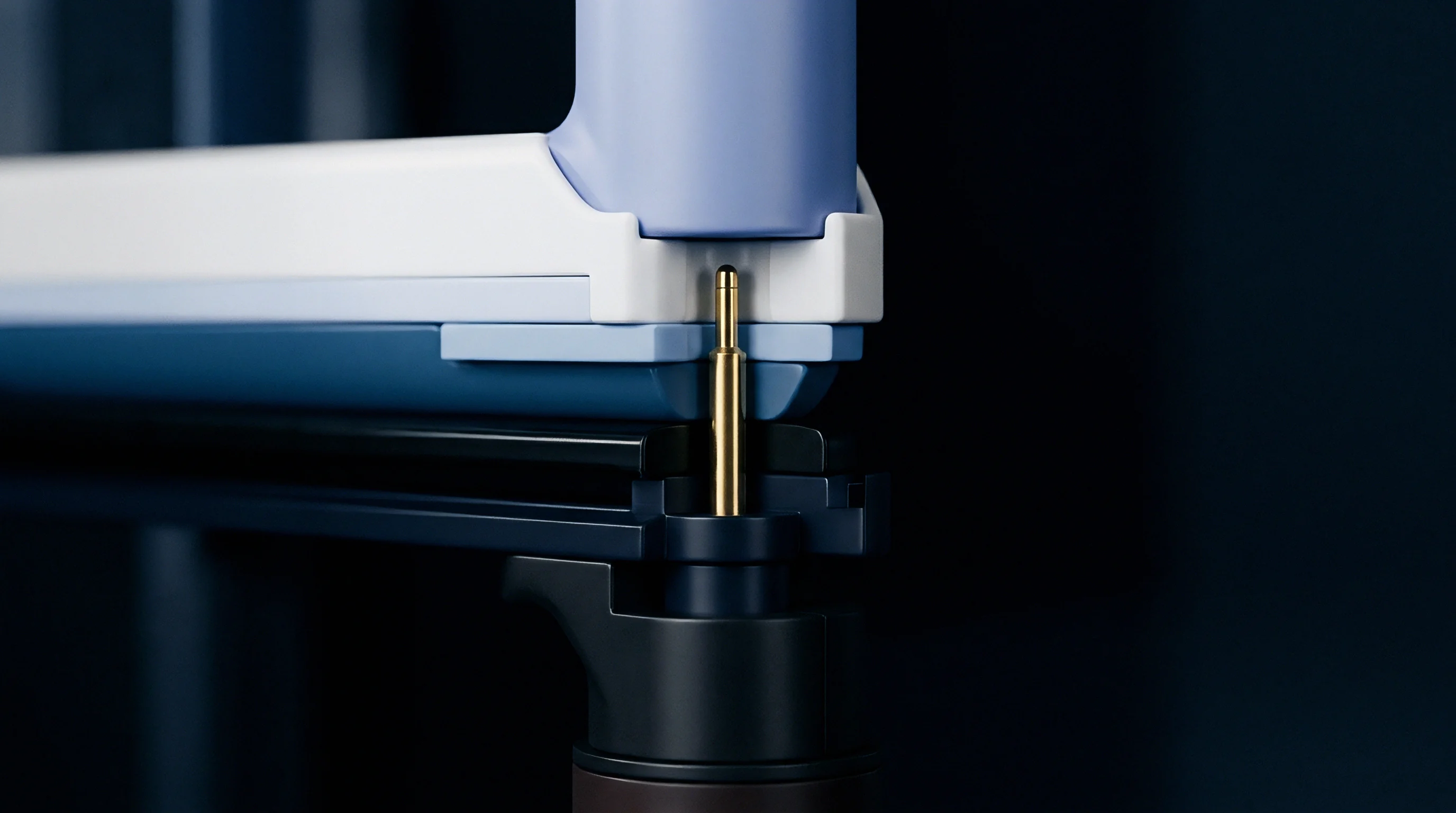

Plunge
Automated continuous screening machines index prismatic, cylindrical, and pouch cells through electrical test stations at rates exceeding 120 units per minute. At these line speeds, mechanical pin drive mechanisms press spring-loaded contact tips onto cell terminals within time windows shorter than 150 milliseconds. The physical velocity of the stroke generates substantial kinetic energy upon mechanical impact.
Mechanical force settings must balance electrical contact stability against surface deformation on the terminal substrate.
High contact impact forces shatter native surface oxides present on nickel-plated steel cans, aluminum tabs, and copper busbars. Force levels between 2.0 N and 6.0 N per pin force tip points through ambient surface films, establishing direct metallic contact bridges required for low-noise measurements. Excessively aggressive drive velocity induces structural bounce, severe tip tip-point flattening, and permanent micro-denting on cell terminal surfaces.
Terminal indentations exceeding 15 micrometers compromise laser welding integrity during subsequent module construction.
| Actuation Drive Mechanism | Contact Velocity (m/s) | Peak Impact Force (N) | Settling Time (ms) | Terminal Denting Depth (µm) |
|---|---|---|---|---|
| Unbuffered Pneumatic Cylinder | 1.20 | 8.5 | 28 | 22.4 |
| Damped Pneumatic Cylinder | 0.65 | 4.8 | 14 | 11.2 |
| Direct Servo Linear Drive | 0.30 | 3.2 | 4 | 4.1 |
| Cam-Driven Mechanical Linkage | 0.45 | 3.8 | 8 | 6.8 |
Pneumatic cylinders operating without velocity control deliver non-linear deceleration profiles. Peak impact energy converts directly into tip plastic deformation and tab gouging. Direct servo linear drives allow programmable soft-landing motion curves, reducing stroke speed to 0.1 m/s in the final millimeter before terminal contact.
This controlled motion minimizes pin rebound, allowing electrical measurement acquisition to begin within 5 milliseconds of touch down.
Spring preload stiffness defines the static contact force maintained during the current pulse. Spring relaxation occurs over millions of duty cycles under continuous high-temperature or high-speed operation. Loss of spring preload reduces interface force below the threshold required to maintain stable surface contact, introducing high-frequency vibration noise into small-signal alternating current impedance measurements.
Setting pneumatic actuation pressures without dynamic load cell validation causes uneven force distribution across multi-pin force-sense crown assemblies, skewing resistance readings across test slots.
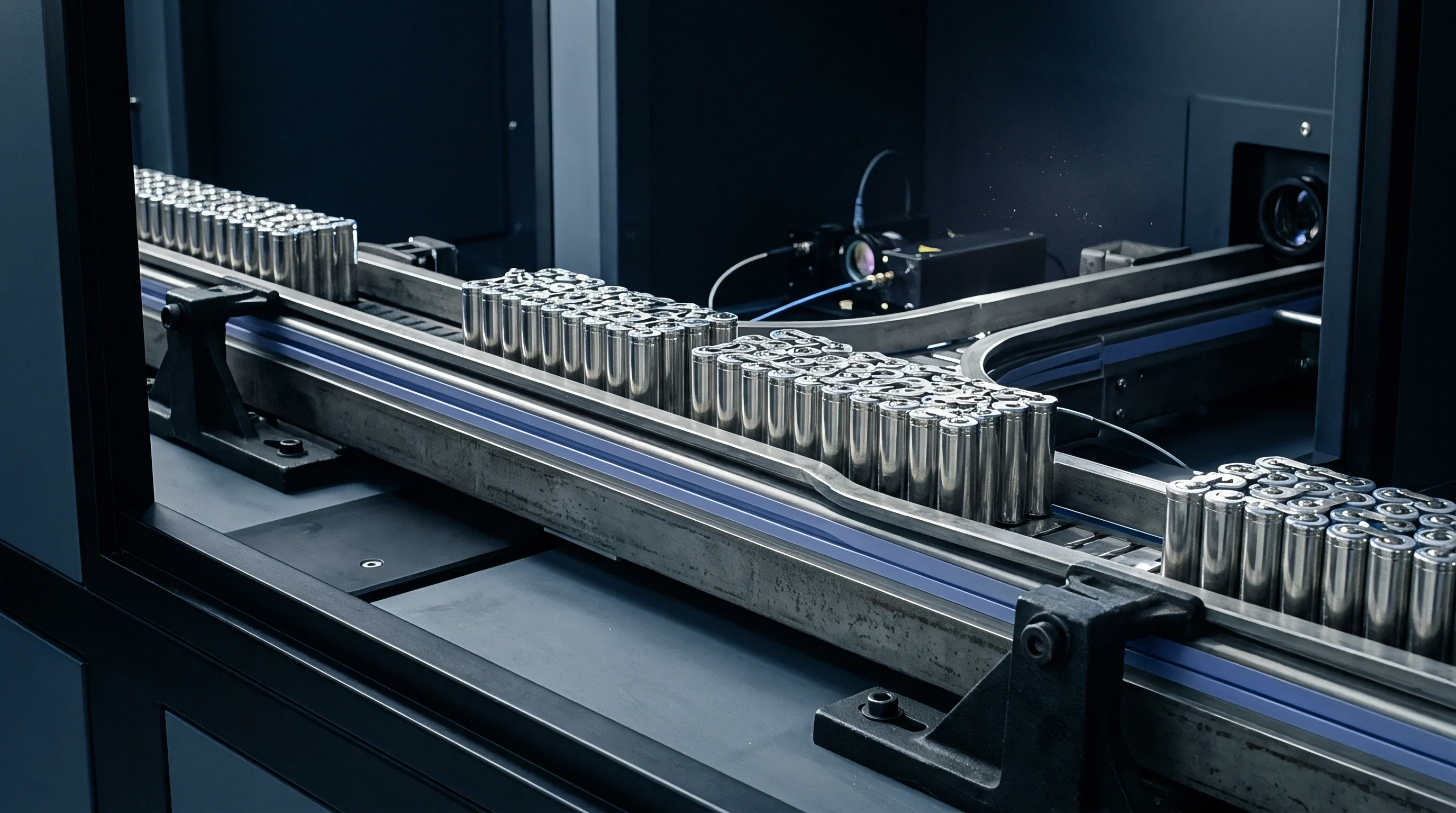
Debris
Continuous contact against cell terminals strips soft metallic species and surface coatings, accumulating loose particles around the test interface. Aluminum transfer from pouch cell tabs onto probe tip points forms insulated aluminum oxide films within several thousand contact cycles. Hard oxide particles imbed into softer tip substrates, creating resistive boundary layers that alter local current density paths.
Fretting wear occurs when machine vibrations induce micro-motion between pin tips and cell terminals during active measurement. Frictional heat drives localized oxidation on beryllium copper and phosphor bronze base metals once thin gold or palladium-cobalt surface platings wear away. Oxide growth increases interfacial contact resistance from a pristine 5 milliohms to over 20 ohms, pushing voltage drop levels beyond instrument tracking limits.
- Intermetallic transfer layer formation alters contact surface chemistry when soft tab material transfers directly to hard probe tips.
- Micro-arcing erosion pits contact points during fast pulsed direct current internal resistance tests when force signals bounce during current flow.
- Organic film build-up traps evaporated electrolyte solvent vapors and drawing oils, forming insulating carbonaceous crusts under repeated local resistive heating.
- Plating spallation exposes underlying reactive substrate metals to atmospheric oxygen after friction strips thin noble metal topcoats.
A pulsed current step of 10 amperes applied across a bouncing Kelvin contact generates local arc temperatures exceeding 1,200 degrees Celsius, vaporizing pin plating materials within 2 milliseconds.
Current timing must synchronize precisely with mechanical contact verification loops. Triggering high-current direct current internal resistance discharge pulses before physical contact stabilization causes micro-arcing across sub-micron air gaps. Arc discharges melt localized tip material, producing microscopic craters and spherical splatter debris.
These burned crater edges act as stress risers, accelerating mechanical tip cracking under subsequent plunging cycles.
Screening machinery operators frequently assume that increasing mechanical actuation force overcomes debris buildup without replacing worn pin hardware. Elevating stroke force onto heavily contaminated probe tips drives hard oxide particles deeper into cell terminal surfaces, causing deep puncturing and metal shearing. The equipment manufacturer insists that probe assemblies perform without maintenance for two million cycles, omitting the reality that soft aluminum tab screening destroys tip conduction pathways within fifty thousand operations.
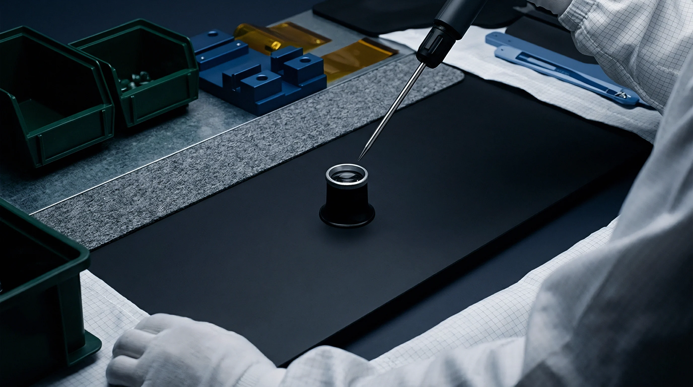
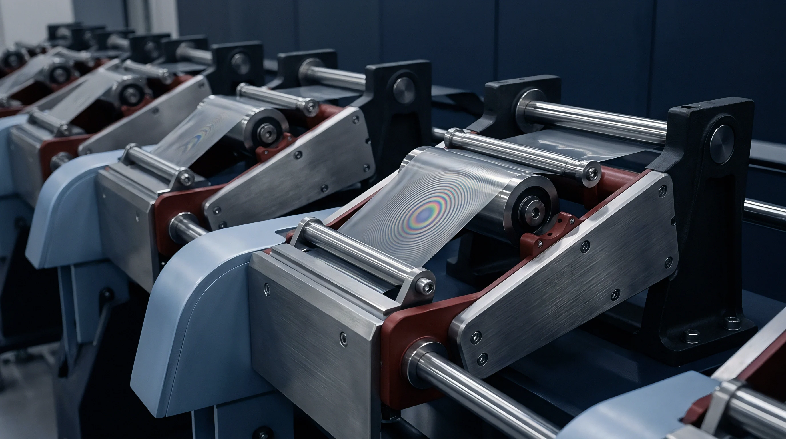
Metrology
Four-wire Kelvin sense configurations eliminate lead and nominal contact resistance from measurement circuits by separating current injection paths from voltage measurement channels. High-input impedance operational amplifiers measure differential voltage drop across the cell terminals while drawing negligible current through sense pins. Severe contact degradation breaks this basic metrological assumption.
When sense contact resistance exceeds tens of ohms due to thick oxide films or trapped debris, the input bias current of sense amplifiers creates a non-negligible voltage drop across the sense pin itself. High contact impedance degrades common-mode rejection ratios, coupling ambient power line noise and servo drive switching frequency interference directly into delicate millivolt signal channels. Alternating current internal resistance measurements conducted at 1 kHz suffer severe phase angle distortion, falsely elevating measured real impedance values by up to fifteen percent.
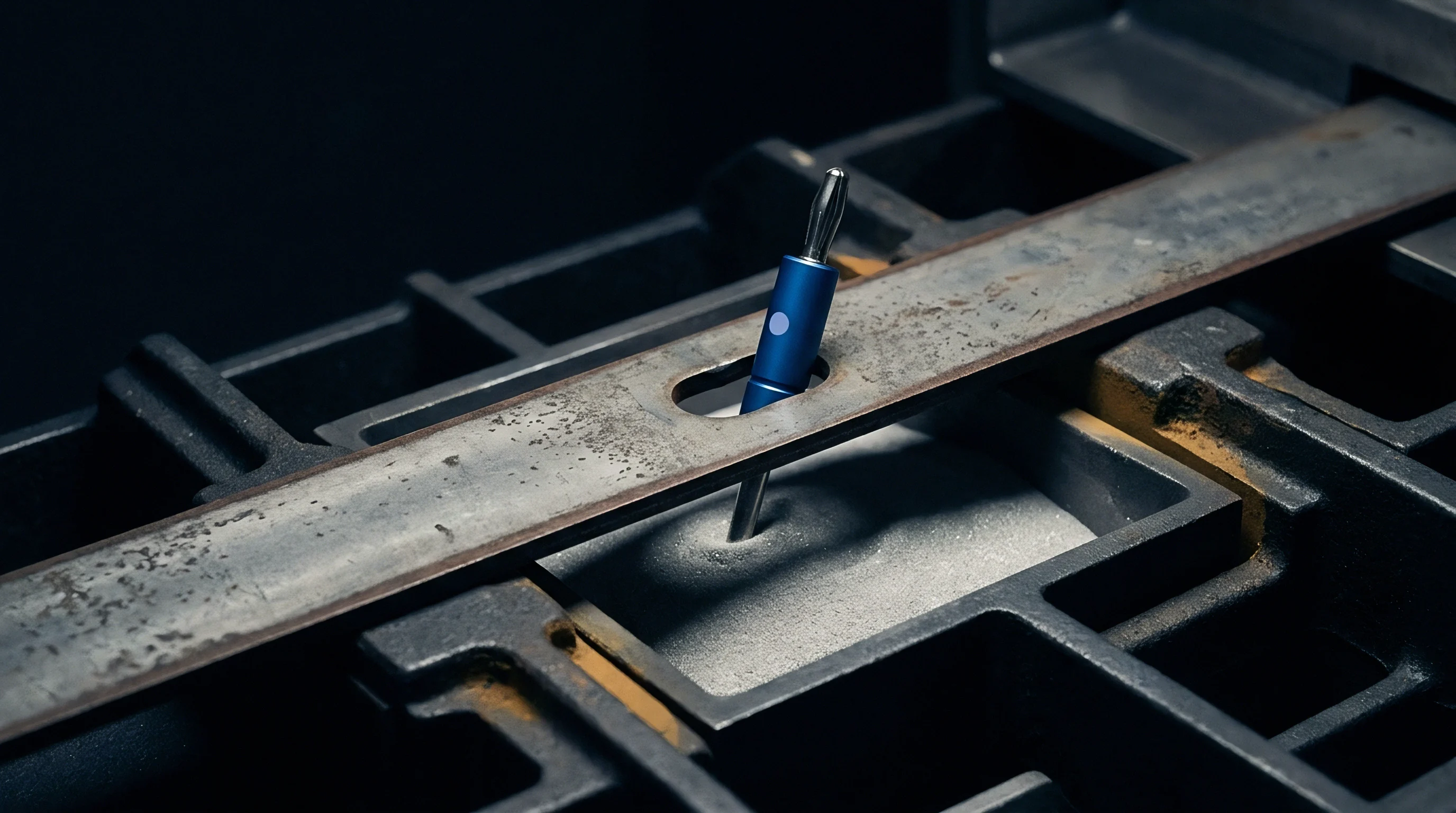
When Should Automated Kelvin Probes Be Retired?
Determining pin replacement schedules relies on tracking contact resistance drift through automated verification loops rather than fixed cycle counts. Continuous open circuit voltage decay screening demands sub-millivolt accuracy over multi-hour monitoring periods to compute reliable capacity loss rates. Degraded sense contacts introduce micro-voltammetric drift and thermal electromotive force spikes, obscuring true electrochemical cell self-discharge signatures.
- Index a gold-plated copper shorting calibration block into the test position every 500 screening cycles.
- Perform a four-point resistance measurement across force and sense lines individually to isolate channel impedance from cell parameters.
- Log the measured isolated line resistance into the line data historian against baseline values established during pin installation.
- Flag individual probe points when channel resistance exceeds 2.5 ohms above initial installation values.
- Trigger an automated pin cleaning sequence or halt the test station channel when channel resistance exceeds 5.0 ohms.
Contact resistance on sense lines exceeding 5.0 ohms degrades instrumentation common-mode rejection, causing false high-impedance cell rejections on cell production lines.
| Tip Substrate & Coating | Hardness (HV) | Electrical Conductivity (% IACS) | Oxidation Resistance | Typical Cycle Life (Aluminum Tab) |
|---|---|---|---|---|
| Beryllium Copper / Hard Gold Flash | 380 | 22 | Moderate | 25,000 |
| Beryllium Copper / Palladium-Cobalt | 600 | 18 | High | 120,000 |
| Tungsten Carbide / Uncoated | 1,500 | 10 | High | 350,000 |
| Tool Steel / Diamond-Like Carbon | 2,200 | 1 | Extreme | 500,000 |
Choice of substrate material dictates tribological endurance and measurement performance. Diamond-Like Carbon coatings yield high mechanical hardness and wear resistance, but their low electrical conductivity limits usage strictly to high-impedance sense pins. Force pins carrying high direct current pulses require high-conductivity substrates such as Palladium-Cobalt over Beryllium Copper to balance electrical ampacity against mechanical deformation resilience.
Ignored sense contact wear causes valid grade-A cells to fail factory screening criteria.
Line calibration routines must measure loop impedance on active test channels continuously.
Cleaning
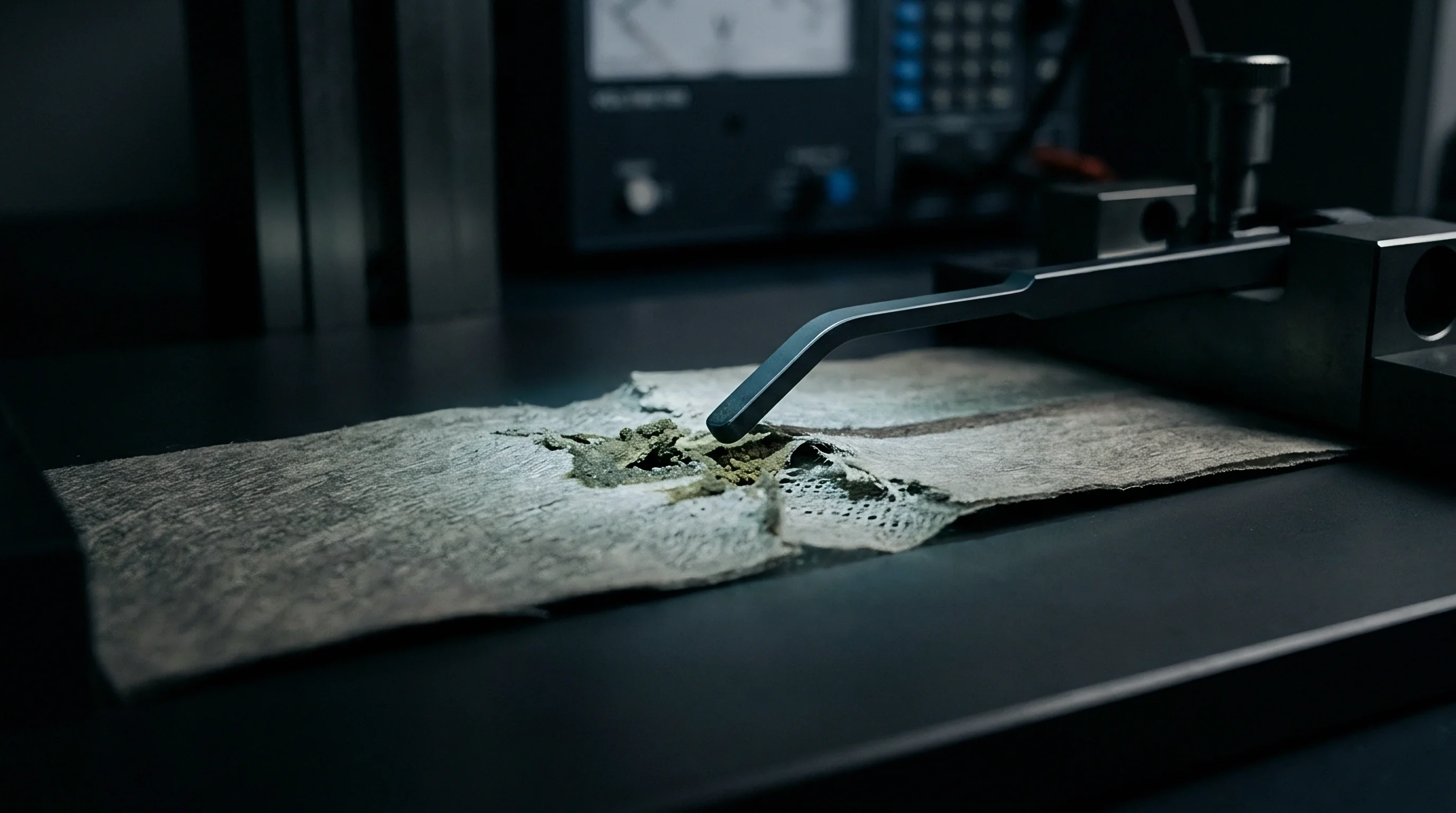
Maintaining probe tips in high-speed automated machinery requires active online surface restoration systems to strip accumulated debris before oxides bond to base metals. Tip geometries dictate debris shedding capability. Single sharp chisel points cut through surface films easily, but concentrate high stress that accelerates tip rounding.
Multi-point crown tips distribute impact force, holding geometry longer while catching loose debris within point recesses.
Automated inline cleaning modules integrate solvent-assisted rotating brush assemblies or micro-abrasive burnishing blocks directly inside the indexing motion path. Cleaning routines actuate probe tips into burnishing media every several hundred cell cycles, removing oxidized surface layers and restoring metallic contact facets. Burnishing operations strip plating layers if stroke counts and contact pressures exceed calibrated thresholds.
- Multi-needle crown geometry provides redundant contact points per channel while trapping loose surface flakes inside center cavity channels.
- Chisel edge geometry breaks heavy surface passivation layers on nickel-plated terminals through shear force application.
- Rotary solvent brushing dissolves organic electrolyte residues and drawing oils using specialized fast-evaporating dielectric solvents.
- Micro-abrasive burnishing blocks remove bonded intermetallic layers through controlled mechanical abrasion during automated maintenance cycles.
A rule of thumb dictates that automated brush cleaning cycles must run twice per shift to prevent soft aluminum transfer from forming permanent intermetallic oxide bonds.
Ultrasonic cleaning baths installed offline provide total debris removal for heavily fouled probe blocks. Removing pin assemblies from screening machines introduces mechanical re-alignment downtime that reduces overall equipment effectiveness. Technicians evaluating online cleaning strategies must determine whether in-situ solvent brushing damages surrounding pneumatic seal materials over long operating campaigns.
Ledger
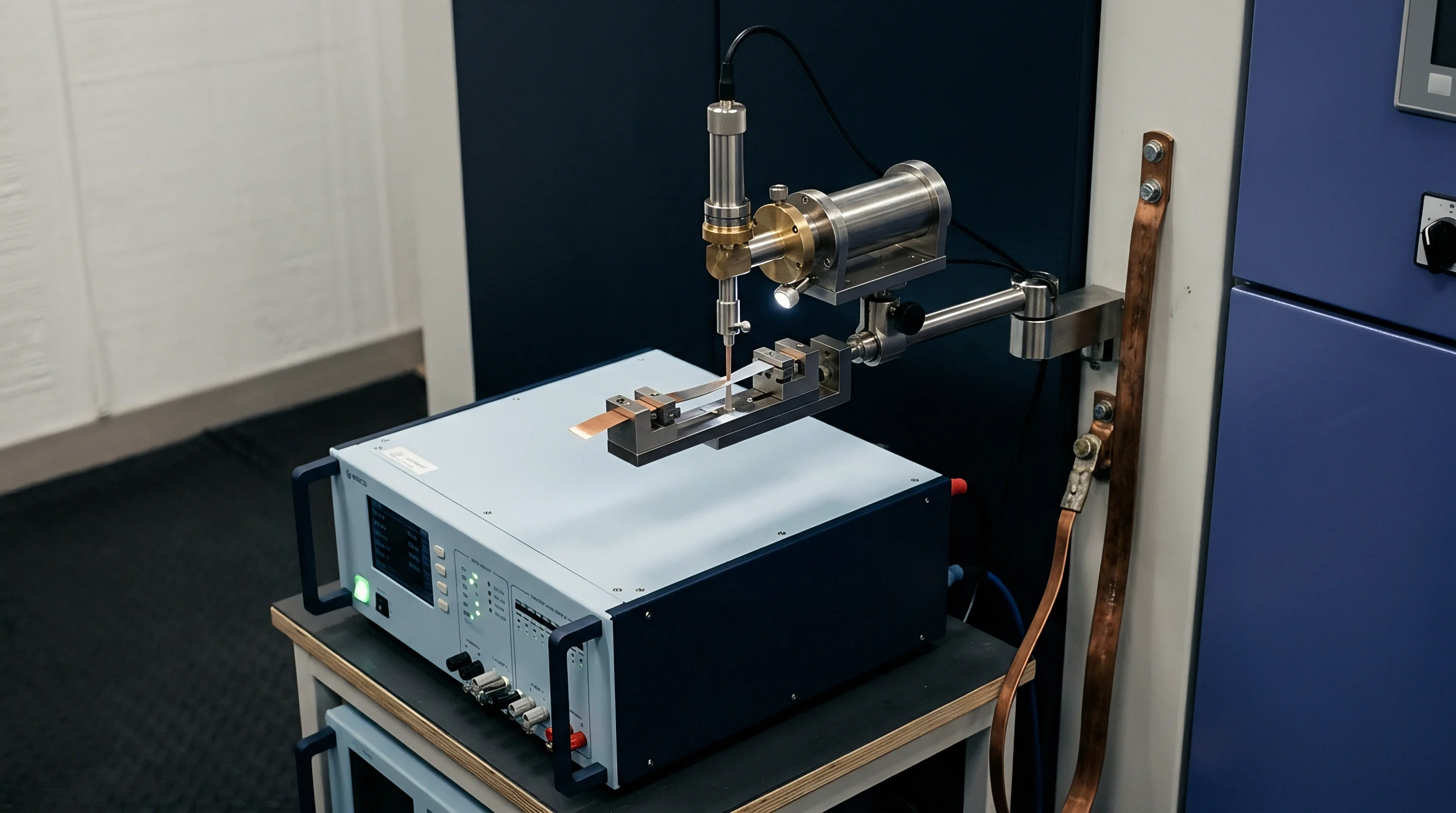
Degraded Kelvin contacts distort screening data, causing direct financial loss through false scrap identification and uncollected field failure exposure. A false reject occurs when a high-quality cell displays falsely elevated internal resistance caused entirely by probe pin oxidation. The test software categorizes the cell as scrap, stripping commercial value from prime inventory.
Scrap costs escalate rapidly in continuous high-volume production facilities processing thousands of cells per hour. A line producing 100,000 units per day with a false reject rate elevated by two percent due to worn test pins generates 2,000 falsely rejected grade-A cells daily. At a cell manufacturing cost of three dollars per unit, poor probe maintenance costs six thousand dollars per line per day in wasted cell scrap alone.
| Operational Parameter | Unmanaged Probe Wear | Scheduled Manual Replacement | Automated Inline Cleaning & Loop Control |
|---|---|---|---|
| False Reject Rate (%) | 3.80 | 0.85 | 0.05 |
| Daily False Scrap Cost (100k units/day @ $3) | $11,400 | $2,550 | $150 |
| Weekly Probe Hardware Cost ($) | $400 | $2,200 | $950 |
| Monthly Unscheduled Line Downtime (Hours) | 18.5 | 4.0 | 0.5 |
| Net Monthly Cost Impact ($) | $358,000 | $82,500 | $7,200 |
Contractual agreements between cell manufacturers and line machinery integrators specify clear performance limits regarding measurement stability and contact hardware longevity. Failure to enforce tip degradation limits transfers warranty liability onto cell pack assemblers, who receive improperly graded cells containing high internal contact resistance undetected by degraded screening rigs.
- Maximum allowable false reject rate clauses cap line scrap attribution to contact pin wear at 0.1 percent of total throughput.
- Automated channel isolation logging requires machinery to store force and sense channel resistance metrics for every single tested unit.
- Mandatory pin replacement thresholds set hard operating cycle limits after which contact spring and tip hardware must be replaced regardless of operational status.
- Calibration shorting block verification obligates line controllers to run physical reference checks prior to resuming production after any line pause.
Quality assurance standards mandate that equipment qualification documentation must contain continuous channel resistance tracking logs for every screening station operating on the factory floor.