Identifying Microsecond Timing Drift in Multi Channel Battery Test Systems
Microsecond timing drift across multi-channel cyclers corrupts DCIR and dQ/dV metrics, requiring hardware-latched PTP clocks to ensure phase alignment.
Clockwork
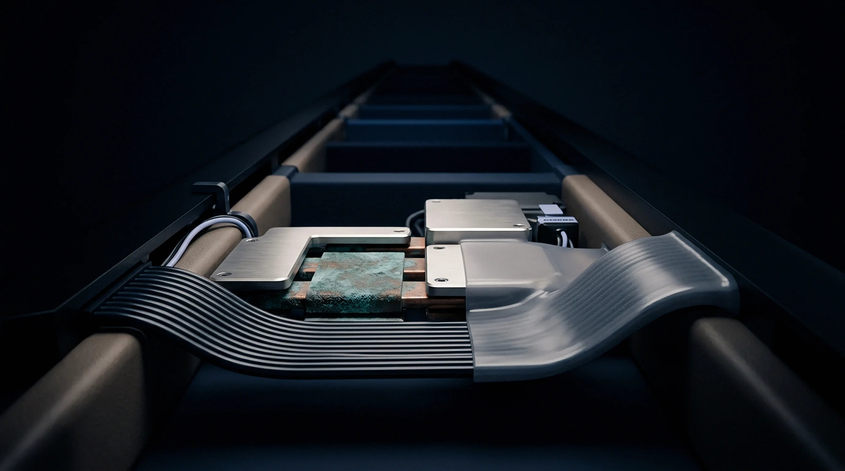
Primary timing references in high-density battery test systems depend on crystal oscillators located on individual channel boards or central system backplanes. These components establish sample latches for Analog-to-Digital Converters (ADCs) and control pulse durations for dynamic load drivers. High-channel-count cyclers divide acquisition across distributed circuit boards, where each board maintains its own local clock distribution tree or receives a divided clock routed across a passive backplane from a central controller.
As channel density increases within a chassis, physical trace length variations and thermal gradients across the backplane introduce nanosecond-to-microsecond temporal offsets between sampling channels.
Thermal variation destabilizes uncompensated quartz crystal oscillators across operating test racks.
Oscillator frequency tolerance is specified in parts per million (PPM) relative to a nominal resonant frequency at twenty-five degrees Celsius. Standard commercial Temperature-Compensated Crystal Oscillators (TCXOs) carry a frequency stability rating from plus-or-minus one PPM to plus-or-minus five PPM across their rated thermal range, whereas uncompensated quartz crystals can drift by more than fifty PPM over a zero-to-seventy degree Celsius envelope. In a multi-channel cycler running high-current profiles, heat dissipated by heat sinks, power MOSFETs, and current shunts drives internal chassis temperatures up unevenly.
Channel card one might sit at thirty degrees Celsius while channel card sixteen reaches fifty-five degrees Celsius. This temperature differential pulls local crystal frequencies apart, causing timer registers to increment at slightly different rates.
Distributed Architecture and Master Timebases
Distributed battery test architectures separate measurement acquisition from central database logging. Local microcontrollers or Field Programmable Gate Arrays (FPGAs) sample current and voltage signals at high rates, buffering measurements in local Static Random-Access Memory (SRAM) before transmitting packetized data to a host controller over an internal bus. Buses such as Controller Area Network (CAN), Inter-Integrated Circuit (I2C), or Ethernet-based protocols like EtherCAT introduce variable transmission latencies tied to packet collisions, interrupt priorities, and buffer queue depths.
Internal thermal gradients alter the baseline frequencies of master timebases.
When host software timestamps incoming data on packet arrival rather than the moment of ADC latch conversion, transmission jitter registers directly in the exported dataset. In test profiles requiring microsecond synchronization across channels, packet-arrival timestamping introduces irrecoverable phase distortion. Systems relying on Network Time Protocol (NTP) over standard Ethernet backplanes achieve synchronization accurate only to within one-to-ten milliseconds ~ falling well short of the sub-microsecond precision required for high-rate pulse power characterization and dynamic impedance spectroscopy.
A temperature variance of ten degrees Celsius across adjacent channel boards induces an oscillator frequency shift exceeding twenty parts per million.
Thermal Coefficients and Crystal Drift Dynamics
Master-slave clock architectures distribute a high-frequency master clock signal across the system backplane to force all ADC sample latches to execute synchronously. Even so, routing clock trees across a multi-slot chassis introduces phase skew from trace capacitance, buffer propagation delays, and impedance mismatches. Signals travel through standard FR-4 circuit board traces at roughly six inches per nanosecond, meaning a twelve-inch routing difference between slot one and slot twelve creates a fixed two-nanosecond propagation delay.
Buffer chips added along the clock tree to maintain drive strength introduce another one to five nanoseconds of delay uncertainty per stage.
Accumulated propagation delays between channels expand over multi-day test runs. If the master timebase drifts with aging or ambient temperature changes, the relative phase offset between channel slots stays fixed in physical time but shifts relative to the ideal clock period. A 14-microsecond offset can develop across adjacent chassis slots during full-load thermal cycling, generating systematic timing errors across channels operating on separate physical cards within the same chassis frame.
Whether lower-cost multi-channel cyclers will adopt oven-controlled crystal oscillators or shift entirely to hardware-switched optical clock networks remains an open technical division among equipment designers.
Skew
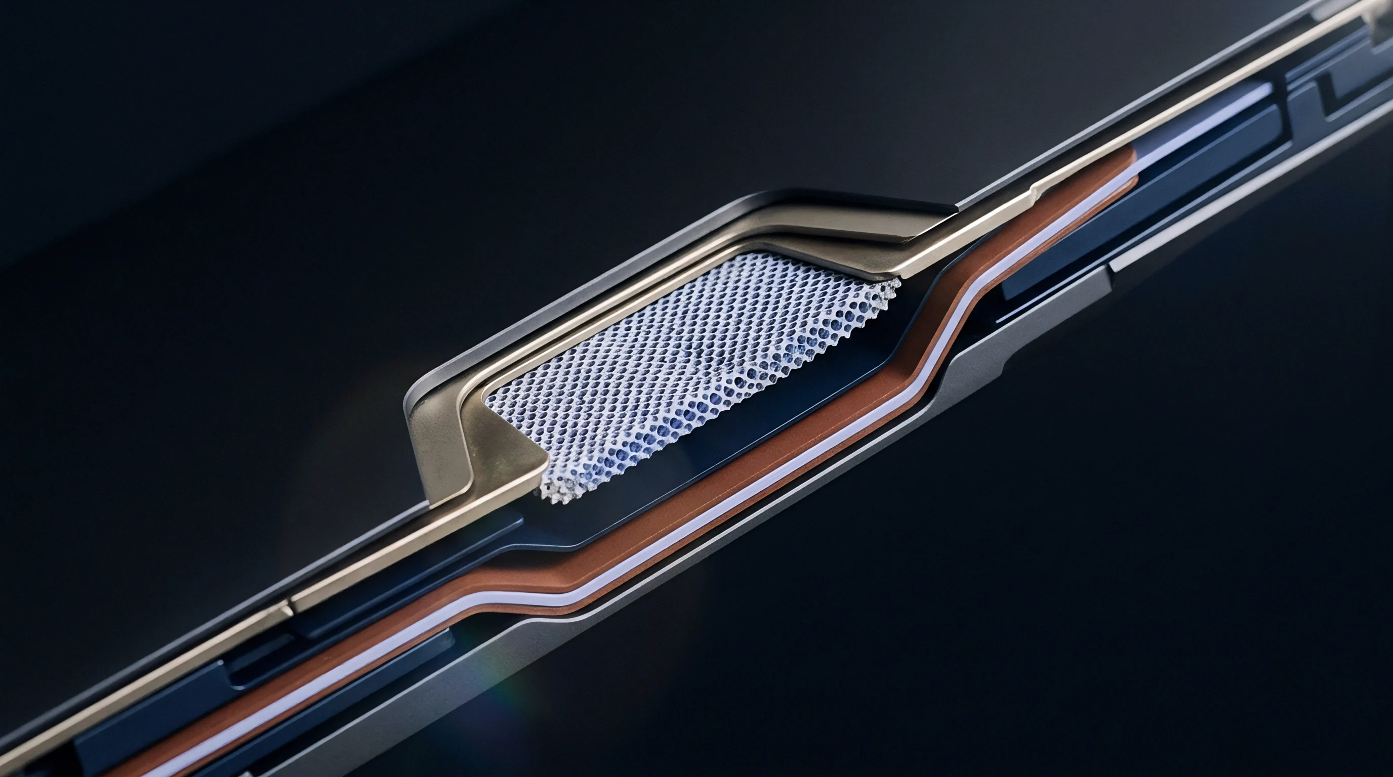
Phase offsets between current command triggers and voltage measurement sample latches introduce systematic errors during fast transient testing. Battery test systems acquire cell voltage and current simultaneously to calculate power, energy, and internal impedance, requiring current and voltage ADCs to latch their inputs at the exact same physical moment. In multi-channel systems, physical isolation and layout constraints often force separate signal paths: differential voltage sense leads wire straight to the cell terminals, while current measurements rely on precision shunts or Hall-effect transducers mounted on high-current busbars.
Acquisition sampling offsets shift the apparent position of capacity peaks.
Analog-to-Digital Converter architectures determine internal conversion delays. Delta-Sigma ADCs use digital decimation filters that impose an inherent group delay between the analog input and the output digital word, often spanning tens of clock cycles depending on filter order and decimation rate. Successive Approximation Register (SAR) ADCs latch the analog signal immediately on a conversion start edge ~ yielding zero group delay, but demanding precise external timing control.
Mixing ADC architectures or filter configurations between current and voltage measurement circuits introduces a fixed, hardware-level acquisition phase delay.
Channel-to-Channel Acquisition Latency
The impact of temporal offset on calculated direct current internal resistance (DCIR) scales directly with the rate of current change (dI/dt). During a Hybrid Pulse Power Characterization (HPPC) pulse, the cycler commands a sharp step current change, driving the cell from zero to one hundred amperes in under one hundred microseconds. Calculated resistance at time t follows Ohm’s Law, where resistance equals voltage change divided by current step magnitude.
If the voltage channel lags current acquisition by fifteen microseconds, the logged dataset pairs the updated current magnitude with an earlier voltage captured before the full ohmic drop develops.
Unmatched filter stages distort transient pulse response curves.
This timing misalignment distorts the calculation of initial ohmic resistance (Rohmic). The recorded voltage appears higher than the actual voltage during a discharge pulse, artificially depressing the calculated DCIR value. On the trailing edge of the pulse, the same phase delay causes the voltage drop to linger after current returns to zero, generating a false residual voltage decay profile.
As pulse durations shorten and transition edges sharpen, microsecond timing offsets shift from negligible phase noise into the primary source of error in internal resistance calculations.
| Pulse Current Step Rate (A/us) | Timing Offset (us) | True Cell Ohmic Resistance (mOhm) | Apparent Measured Resistance (mOhm) | Calculated Resistance Error (%) |
|---|---|---|---|---|
| 1.0 | 2.0 | 0.500 | 0.480 | -4.00 |
| 1.0 | 10.0 | 0.500 | 0.400 | -20.00 |
| 5.0 | 2.0 | 0.500 | 0.400 | -20.00 |
| 5.0 | 10.0 | 0.500 | 0.100 | -80.00 |
| 10.0 | 1.0 | 0.200 | 0.150 | -25.00 |
| 10.0 | 5.0 | 0.200 | -0.050 | -125.00 |
| Data assumes step pulse profile with linear current ramp rate and instantaneous ohmic cell response. Negative apparent resistance indicates voltage sampled prior to current edge development. | ||||
Analog Filter Phase Shift and Digital Latch Times
Low-pass analog filters placed at ADC inputs prevent high-frequency switching noise from aliasing into the measurement band. These passive RC networks introduce phase shift, attenuating high-frequency noise while delaying low-frequency voltage and current waveforms. Passive component tolerances govern this phase response directly: commercial capacitors carry tolerances of plus-or-minus five or ten percent, while resistors typically carry one percent tolerances.
Discrepancies in analog filter delays generate channel-to-channel phase errors.
A ten percent deviation in input filter capacitance shifts the cutoff frequency (fc), altering group delay for signals passing through that channel. If a voltage sense line uses a 10 kOhm resistor and a 100 nF capacitor (fc = 159.1 Hz), the nominal time constant (τ) equals one millisecond. A ten percent increase in capacitance extends the time constant to 1.1 milliseconds.
This one hundred microsecond difference in analog filter delay between adjacent channels creates artificial temporal drift, breaking real-time phase matching across parallel cell channels even when digital sample triggers are synchronized at the converter latches.
Asymmetric low-pass filter cutoff frequencies between voltage and current sense lines introduce phase delays that mimic electrochemical charge-transfer resistance.
Matching anti-aliasing filter passive component tolerances yields greater reduction in timing offset than over-sampling with uncalibrated high-speed converters.
Diagnostic
Verifying temporal alignment across multi-channel battery test platforms requires external, high-bandwidth reference instruments connected directly to internal board test points. Standard battery cycler export files lack the precision to reveal microsecond timing offsets, as host software averages or truncates timestamp data to millisecond resolution. Hardware diagnostics isolate phase errors down to the converter latch and trigger distribution level.
Direct probing across precision shunts captures the true voltage dynamics.
Timing skew is evaluated using parallel probe taps connected to high-speed digital storage oscilloscopes (DSOs) or dedicated Time-Interval Counters (TICs). Connecting channel one and channel sixteen to an external reference step signal reveals offsets between individual channel cards. A high-bandwidth arbitrary waveform generator injects a synchronous square-wave voltage pulse into the sense leads of all channels under test.
The oscilloscope captures the resulting conversion start signals, ADC latch pulses, and interrupt lines, displaying temporal offsets between distinct channel slots on a unified time base.
Can Microsecond Timing Drift Distort Pulse Resistance Measurements?
Microsecond timing drift degrades short-duration pulse power characterization profiles by misaligning the current command edge with the observed voltage response. In battery dynamic characterization protocols, pulse durations range from ten milliseconds to ten seconds, with sampling rates set to ten kilohertz or higher. When microsecond temporal skew exists between current generation and voltage measurement, the rapid initial voltage drop governed by pure ohmic resistance is captured out of sequence.
This causes calculated DCIR values to drift across test runs, producing false variations in internal resistance data that reflect test channel electronics rather than cell degradation.
Nominal data acquisition rates frequently conceal hardware-level conversion latencies.
Determining whether observed timing offsets originate from hardware drift or software buffer handling requires a systematic diagnostic approach. The test bench setup must bypass host communication layers to monitor raw hardware signals directly at the circuit board edge.
- High-Bandwidth Oscilloscope Probing directly monitors physical ADC conversion-start signals on adjacent channel cards to quantify clock distribution trace delay and buffer propagation skew.
- Precision Step Waveform Injection feeds a nanosecond rise-time current impulse across all current shunts to measure physical acquisition phase lag across the full multi-channel array.
- Time-Interval Counter Analysis logs frequency drift on local crystal oscillators across extended thermal cycles to compute individual parts-per-million frequency variations.
- Hardware Trigger Line Verification confirms that backplane synchronization pulses arrive at distinct channel slots within allowable sub-microsecond arrival windows.
- Decimation Filter Group Delay Mapping tracks phase delay variations between different ADC firmware builds and decimation filter configurations across cards.
Acquisition phase lag introduces cumulative errors into numerical current integration.
Hardware-level diagnostic routines must run under active thermal load. Testing timing integrity while channels sit idle masks frequency shifts caused by heat dissipation from internal power electronics. Running all cycler channels at maximum charge and discharge currents elevates internal chassis temperatures, driving local crystal oscillators into their maximum thermal frequency deviation.
Oscilloscope measurements recorded during peak thermal stability yield the definitive operational timing drift profile for the multi-channel array under test.
Compliance with standardized battery pulse characterization mandates verified signal synchronization across all active test lines before data qualification.
Unresolved channel acquisition delays lead directly to rejected cell qualification reports, forced re-testing of production batches, and invalidation of supplier warranty claims.
Error
Calculated electrochemical metrics suffer structural distortion when underlying time vectors drift during continuous high-rate data logging. Advanced battery health diagnostics rely on exact mathematical derivatives of logged current and voltage datasets over time. Differential Capacity (dQ/dV) and Differential Voltage (dV/dQ) analysis transform smooth charge and discharge curves into detailed peak profiles, exposing internal degradation mechanisms such as active material loss, lithium plating, and solid electrolyte interphase (SEI) growth.
These analytical methods require exceptional timestamp accuracy; temporal noise or sample rate instability introduces mathematical artifacts that mask subtle electrochemical phase transitions.
Uncompensated clock skew undermines the validity of dynamic pulse testing.
In Differential Capacity analysis, capacity increment (Δ Q) is computed as current multiplied by time step (Δ t). The calculated derivative (dQ/dV = I · Δ t / Δ V) depends directly on the stability of the timestamp delta between consecutive sample points. If microsecond timing drift causes acquisition intervals to fluctuate randomly or jump periodically, calculated dQ/dV values experience high-frequency spike noise.
This mathematical noise forces analysts to apply aggressive digital smoothing filters, such as Savitzky-Golay filtering, which flatten genuine physical peaks and obliterate early indicators of cell failure.
| Sampling Interval Stability (us Jitter) | Applied Smoothing Window (Points) | dQ/dV Peak Height Error (%) | Calculated Peak Full-Width Half-Max Shift (mV) | False Noise Spike Amplitude (Ah/V) |
|---|---|---|---|---|
| 0.1 | 5 | 0.02 | 0.10 | 0.001 |
| 1.0 | 5 | 0.15 | 0.40 | 0.012 |
| 10.0 | 10 | 1.20 | 1.80 | 0.105 |
| 50.0 | 20 | 4.80 | 5.20 | 0.450 |
| 100.0 | 50 | 12.50 | 11.40 | 1.200 |

Differential Capacity Analysis Peak Shifts
High-Precision Coulometry (HPC) demands extreme clock stability over weeks or months of continuous cycling. Coulombic Efficiency (CE) measures the ratio of discharge capacity to charge capacity (CE = Qdischarge / Qcharge). Evaluating degradation trends in long-term testing requires resolving CE changes down to the fourth decimal place (99.99% efficiency).
Capacity calculations integrate current over time using trapezoidal numerical integration (int I dt).
Coulombic efficiency calculations depend strictly on high-accuracy timebase stability.
If a multi-channel cycler’s master clock drifts by ten PPM over a thirty-day test run, integrated discharge time expands or contracts relative to physical time. A constant current discharge running over ten hours accumulates a timing offset of 360 milliseconds. While 360 milliseconds appears small relative to ten hours, the resulting integrated ampere-hour calculation shifts by an amount greater than the subtle capacity decay signals associated with side-reaction degradation.
When adjacent test channels drift in opposite directions due to local board temperatures, comparative cell degradation studies become invalid, as channel timing drift obscures real electrochemical differences between chemistry samples.
High Precision Coulometry Integration Artifacts
Timing drift introduces computational errors into power and energy calculations. Energy (E) is computed as the integral of instantaneous power over time (int V · I dt). Misalignment between current and voltage vectors caused by channel-to-channel timing skew introduces an artificial phase angle (thη) between measured signals.
In dynamic load profiling, such as drive cycle simulation (Worldwide Harmonized Light Vehicles Test Procedure, or WLTP), rapid power fluctuations occur continuously across sub-second intervals.
Hardware triggers prevent channel-to-channel acquisition delays across backplanes.
Oscillators drift as rack temperatures swing during high-power dynamic testing runs. Calculated energy transfer during aggressive charge and discharge pulses deviates from actual energy transfer when V and I samples are offset by microsecond intervals. The resulting power integration error causes incorrect estimation of pack thermal generation rates and distorts energy efficiency benchmarking across parallel cell designs.
- False Ohmic Resistance Spikes occur when voltage acquisition lags rapid current transitions during HPPC pulse steps.
- Differential Capacity Peak Broadening emerges when timestamp jitter forces the use of aggressive digital smoothing filters across dQ/dV datasets.
- Coulombic Efficiency Baseline Drift develops as long-term crystal oscillator frequency variations alter calculated integration time bases.
- Spurious Phase Shifts in Dynamic Impedance Data develop when acquisition skew creates artificial time delays between alternating voltage and current waveforms.
- Energy Balance Accounting Inaccuracies arise from misaligned current and voltage sample pairs during high-frequency dynamic drive cycles.
High precision coulometry calculations fail to resolve micro-ampere-hour degradation trends when current sampling intervals fluctuate unpredictably.
Equipment manufacturers frequently attribute observed phase mismatches to external cable inductance or cell busbar reactance rather than internal acquisition backplane delays.
Correction
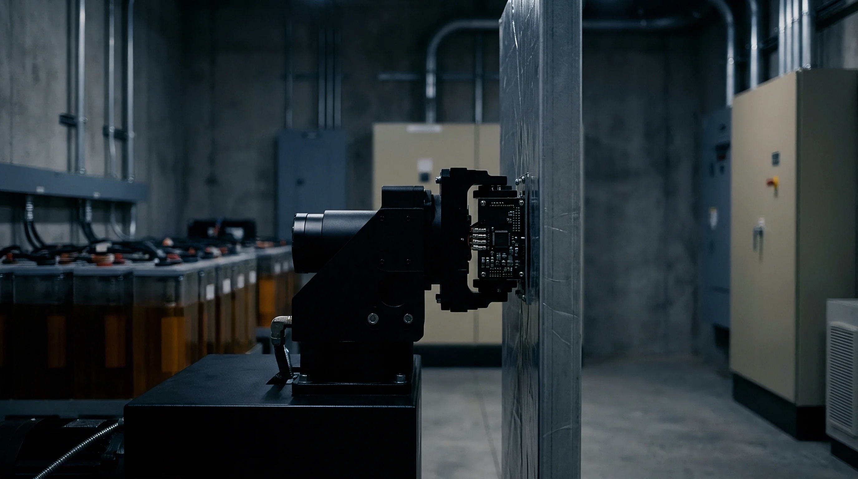
Architectural redesigns and active software compensation protocols establish temporal integrity across high-density test channels. System developers resolve microsecond drift by replacing non-synchronized local clocks with tightly coupled hardware synchronization backplanes. Modern high-precision cyclers deploy Precision Time Protocol (IEEE 1588 PTP) hardware engines integrated directly into the media access control (MAC) layer of backplane Ethernet transceivers.
IEEE 1588 PTP achieves sub-microsecond synchronization across distributed nodes by exchanging hardware-timestamped timing packets, continuously calculating and adjusting for propagation delay and clock drift across active channel cards.
Synchronized clock trees resolve multi-channel timebase drift across dense backplanes.
Hardware-level synchronization relies on dedicated clock distribution networks routing equalized trace lengths from a single master oscillator to all converter latches. Utilizing low-jitter clock fanout buffers ensures that conversion start pulses arrive at every ADC in the chassis within sub-nanosecond time windows. Combining centralized clock distribution with Oven-Controlled Crystal Oscillators (OCXOs) or atomic rubidium references stabilizes the master timebase against thermal fluctuations, driving system frequency stability down to sub-part-per-billion levels over extended testing duration.
Hardware Latched Conversion and IEEE 1588 Implementation
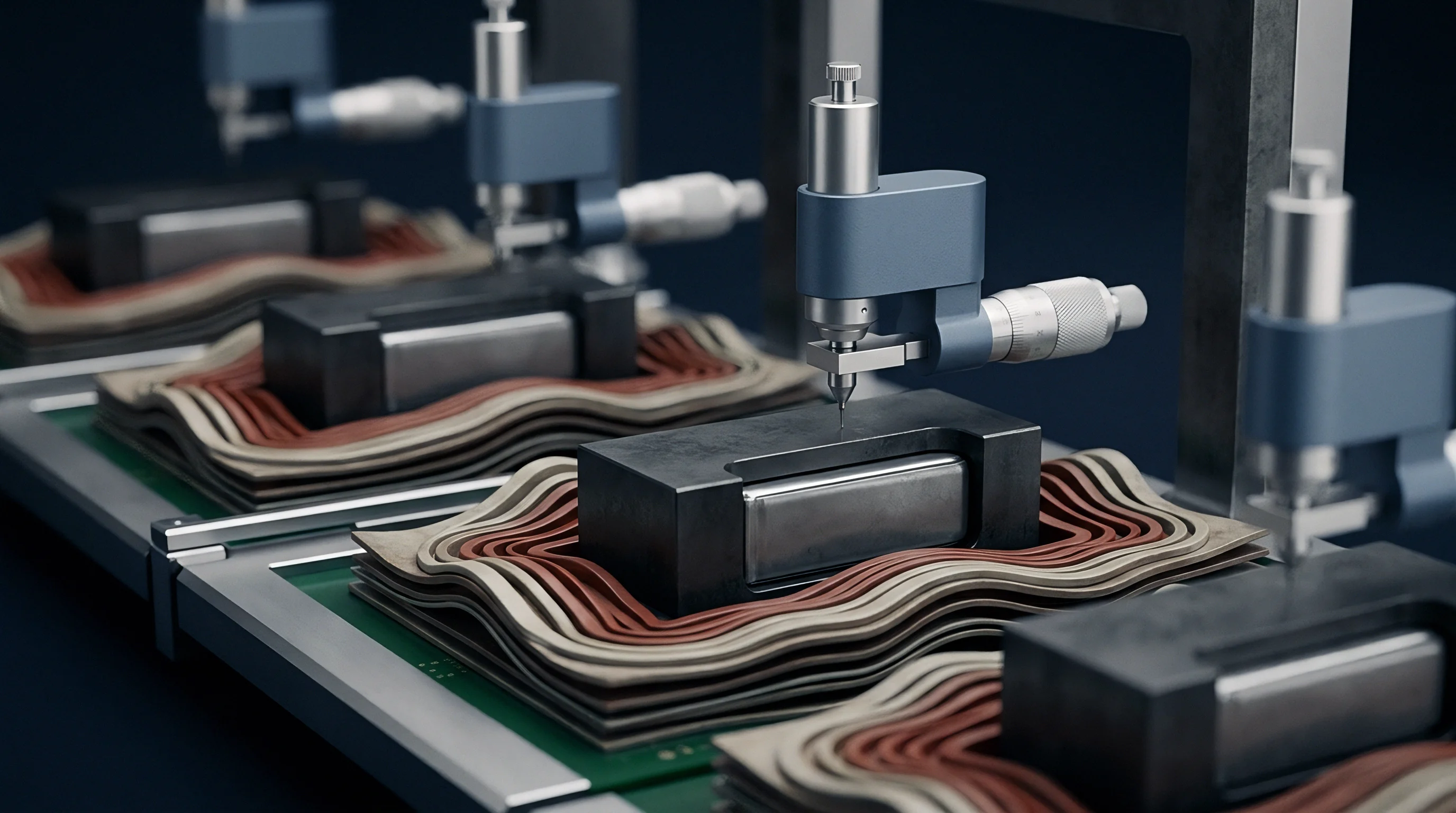
Software post-processing algorithms offer a complementary pathway to compensate for fixed phase delays and residual timing skew in existing test hardware datasets. Linear phase alignment algorithms analyze time displacement between current triggers and initial voltage responses, applying fractional delay filters to re-align voltage and current time-series arrays prior to differential capacity or impedance calculations. Interpolation routines using cubic splines reconstruct missing or jittered data points onto an absolute, uniform physical time grid.
Post-acquisition phase alignment algorithms can partially reconstruct misaligned data streams.
Post-processing software cannot reconstruct high-frequency signal content lost due to physical phase jitter during acquisition. Post-test mathematical correction serves as a secondary fix for historical datasets; primary accuracy requires hardware-enforced simultaneity at the physical converter layer during test execution.
Software Post Processing Phase Realignment
Hardware upgrades and calibration procedures secure long-term timing accuracy across multi-channel facilities.
- Disconnect all external battery channels and connect a calibrated nanosecond rise-time reference pulse generator to the voltage and current acquisition taps.
- Command a synchronized multi-channel step acquisition sequence through the central cycler controller software.
- Capture raw converter latches across all channel slots using a high-speed digital storage oscilloscope tied to the master reference pulse.
- Measure the temporal delay between current and voltage conversion start edges across each physical slot.
- Update firmware calibration registers with individual channel phase offset correction values to align acquisition latches.
- Verify drift-free operation by subjecting the chassis to a four-hour full-load thermal stress cycle while continuously tracking timing stability.
Hardware-triggered ADC capture prevents software interrupt delays from corrupting precision time-series logs.
Contractual procurement specifications for high-density battery test arrays must define cross-channel acquisition simultaneity tolerances under full dynamic thermal loads, forcing suppliers to demonstrate compliance using verified IEEE 1588 clock networks and hardware-latched sampling circuits.