Standardized Verification Protocols for Busbar Surface Plating Integrity
Busbar surface plating integrity requires verified multi-layer thickness control, low internal stress, and zero-defect adhesion to prevent joint degradation.
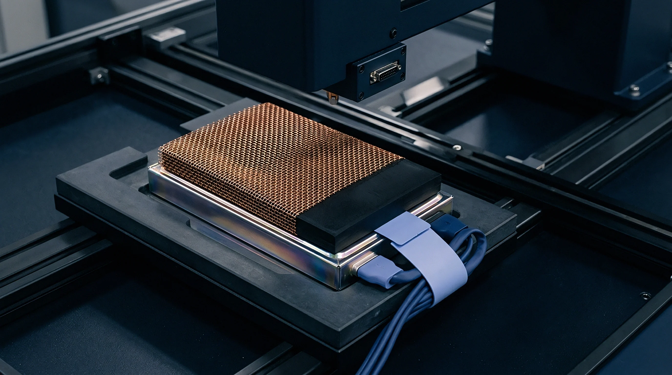
Plating
Electroplated nickel over a copper base provides the standard foundation for high-current battery interconnects. Electrolytic copper delivers the necessary electrical conductivity, with volume resistivity around 1.68 microhm-centimeters at 20 degrees Celsius, but bare metal oxidizes quickly on contact with air. The resulting cuprous and cupric oxide films drive up contact resistance across bolted interfaces and ultrasonic wedge welds, triggering localized ohmic heating during sustained high-rate discharge.
As a result, engineering specifications consistently require barrier coatings to preserve interface conductivity and isolate the copper from atmospheric moisture, ionic residues, and airborne sulfur.
The choice between electrodeposited bright nickel, electroless nickel-phosphorus (ENP), matte tin, or flash silver depends primarily on joint assembly methods and thermal limits. Bright nickel baths use organic brighteners and leveling agents like sulfur-bearing saccharin, which leave residual tensile stresses of 150 to 300 megapascals in the plate. Under mechanical forming or high-energy laser welding, that built-in stress frequently relieves itself through micro-cracking.
Electroless nickel-phosphorus avoids the high-current-density buildup that electrolytic baths produce on stamped edges and fastener holes, depositing an even layer over complex shapes. Formulations with 6 to 9 percent medium phosphorus yield an amorphous or microcrystalline deposit with negligible magnetic permeability, hardness above 500 Vickers, and dependable performance in salt-spray trials.
Elevated operating temperatures make intermetallic growth kinetics the governing factor in long-term joint stability. Without an intermediate barrier layer, tin applied directly over copper undergoes continuous solid-state reaction: copper atoms diffuse into the tin deposit, forming Cu6Sn5 (Eta-phase) and Cu3Sn (Epsilon-phase) intermetallics at rates governed by Arrhenius kinetics. As these brittle phases thicken, contact resistance climbs and Kirkendall voids cluster at the substrate interface due to differential diffusion rates.
Placing 2.0 to 5.0 micrometers of nickel between the copper and tin slows this migration significantly, dropping intermetallic growth rates by roughly two orders of magnitude at continuous 65 degrees Celsius operation.
| Plating Layer Architecture | Nominal Coating Thickness (µm) | Initial Contact Resistance (mΩ·cm²) | Hardness Range (HV) | Thermal Limit (°C) |
|---|---|---|---|---|
| Matte Nickel (Electrolytic) | 3.0 – 8.0 | 0.12 – 0.18 | 150 – 250 | 300 |
| Electroless Nickel (6-9% P) | 5.0 – 12.0 | 0.25 – 0.35 | 500 – 600 | 250 |
| Matte Tin over Nickel Barrier | 5.0 (Sn) / 3.0 (Ni) | 0.04 – 0.08 | 12 – 20 (Sn outer) | 150 |
| Silver Flash over Nickel Barrier | 1.5 (Ag) / 3.0 (Ni) | 0.01 – 0.03 | 70 – 110 | 200 |
Laser welding introduces its own metallurgical constraints. When joining aluminum to copper busbars with an infrared laser, the thickness of any underlying nickel barrier must be kept under close control: exceeding 6.0 micrometers allows surplus nickel into the melt pool, shifting the ternary equilibrium toward brittle Al3Ni and Al3Ni2 phases. At high volumes, these intermetallics degrade weld fatigue life under the vibration spectra outlined in ISO 16750-3.
Conversely, ultrasonic wedge bonding of aluminum wire to nickel-plated busbars requires a matte finish essentially free of organic bath residues to allow solid-state atomic contact at the weld interface.
Coating distribution varies widely between rack electroplating and chemical deposition tanks. In electrolytic baths, field lines concentrate around sharp corners and cut edges, pulling current density upward and building deposits up to three times nominal target thickness while blind holes and internal radii receive marginal coverage. Autocatalytic electroless reduction sidesteps this dynamic entirely, holding thickness within 0.5 micrometers across the whole part geometry.
Operating these baths requires continuous monitoring of solution temperature, pH, and dissolved metal concentrations to prevent bath collapse or stress pitting.
Plating discontinuities undermine the barrier integrity of the entire deposit. When cathodic hydrogen bubbles lodge against the copper surface during electrodeposition, they leave pinholes, gas pits, and nodular artifacts in their wake. A pinhole creates an unfavorable galvanic couple: a tiny copper anode exposed to air and moisture, ringed by a broad nickel cathode.
Any condensed humidity that enters the cavity accelerates base-metal oxidation, and the resulting corrosion products expand beneath the plating until the surrounding layer flakes away and joint contact degrades.
Plating thickness variations exceeding 1.5 micrometers across a 100-millimeter bar increase local electrical resistance by 14 percent after 500 thermal cycles between minus 40 and 85 degrees Celsius.
Adhesion of electroplated metals depends almost entirely on the quality of the initial surface preparation. Stamping lubricants, copper oxides, and mechanical polishing debris isolate the substrate lattice from incoming electrolyte ions. Standard pre-treatment pairs solvent degreasing with an alkaline electro-cleaner to strip organics, followed by a sodium persulfate micro-etch to create mechanical tooth on the copper.
Incomplete oxide stripping leaves a weak boundary layer, inviting interfacial separation when the busbar experiences thermal shock during rapid cell discharge or mechanical twist during module assembly.
Pack manufacturing exposes plated copper to several thermal spikes. Processes like reflow soldering, ultrasonic joining, and structural adhesive baking subject parts to temperatures between 120 and 260 degrees Celsius. In electroless nickel deposits containing medium or high phosphorus, temperatures past 300 degrees Celsius initiate crystallization, precipitating Ni3P phases within the amorphous matrix.
This precipitation drives deposit micro-hardness past 900 Vickers, reducing ductility and making the plating vulnerable to brittle cracking during dynamic shock and drop tests.
Residual internal stresses present real operational risks in heavy-duty commercial vehicle packs. If bath chemistry drifts, internal deposit stresses can exceed interfacial bond strength, producing micro-spalling during field thermal cycling. Flakes shed from spalling busbars migrate through module enclosures, where they can bridge adjacent cell terminals, establish electrical leakage paths, and elevate passive discharge rates.

Grain
Deposit microstructure governs mechanical compliance, toughness, and grain-boundary diffusion throughout the plating layer. Crystalline grain diameter, orientation, and texture reflect bath composition, current density, organic additives, and post-plate thermal history. Coarse equiaxed grains offer lower intrinsic bulk resistivity, whereas fine columnar or nanocrystalline arrangements yield higher yield strength through Hall-Petch boundary strengthening.
Adjusting bath operating parameters allows suppliers to tailor this morphology to the mechanical demands of cylindrical, pouch, or prismatic battery interconnects.
Whisker formation remains a persistent failure mode where matte tin sits over copper conductors. These monocrystalline filaments emerge spontaneously from the tin surface, reaching lengths of several millimeters with diameters between 1 and 5 micrometers. The thermodynamic driver is compressive stress inside the tin layer, generated by interfacial Cu6Sn5 growth, differential thermal expansion between tin and copper, terminal bolt torque, and residual electrodeposition stress.
Because whiskers sustain currents up to 10 milliamperes before fusing open, they create intermittent short circuits across closely spaced BMS traces and voltage-monitoring leads.
Suppressing whisker growth requires tight control over deposit metallurgy and post-plate processing. Switching to a matte tin chemistry that yields larger grains (1.0 to 5.0 micrometers) reduces grain-boundary area, slowing the diffusion pathways that feed whisker growth compared to sub-micron bright tin finishes. A nickel underlayer of at least 3.0 micrometers blocks copper migration into the tin layer, cutting off the Cu6Sn5 growth that generates internal compression.
Annealing plated parts within 24 hours of deposition ~ holding them at 150 degrees Celsius for two hours ~ relieves residual lattice strain and stabilizes the boundary network against spontaneous filament formation.
Surface topography largely dictates how bolted busbar interfaces behave mechanically. Profilometry metrics like arithmetical mean deviation (Ra) and peak-to-valley depth (Rz) determine the real contact area under clamping load. Because surfaces meet only at microscopic high points, apparent contact area is much larger than true load-bearing area.
A rough surface (Ra above 1.6 micrometers) focuses clamping force onto isolated asperities, causing localized yield in soft tin coatings. This plastic deformation ruptures thin surface oxides and establishes low-resistance metallic contact spots.
High surface roughness becomes a liability under ongoing vibration. Tall asperity peaks yield under cyclic micro-motion, generating fretting wear across the interface. The resulting oxidized debris packs into surface valleys, gradually increasing contact resistance and raising operating temperatures under sustained high-current draws.
Maintaining an Ra between 0.4 and 0.8 micrometers, paired with a malleable surface layer like matte tin or silver, allows initial oxide breakdown while mitigating fretting oxidation under cyclic vehicle vibration.
Grain boundaries also act as primary diffusion channels for aggressive environmental contaminants. The high boundary density of fine or nanocrystalline deposits speeds the ingress of atmospheric sulfur, chlorine, and oxygen. Gaseous hydrogen sulfide (H2S) penetrates down boundary networks to react with underlying copper or silver, producing Cu2S or Ag2S corrosion filaments.
Because these sulfide corrosion products are poor conductors, joint resistance rises and battery management systems eventually register localized overheating warnings.
Thermal treatment after electrodeposition reorganizes grain boundaries and relieves internal micro-strain. Annealing electrolytic nickel between 200 and 400 degrees Celsius induces recrystallization, shifting fine columnar structures toward larger equiaxed grains. This thermal soak drops internal lattice stress from over 200 megapascals to under 30 megapascals, noticeably improving flexural fatigue resistance.
Heat-treatment temperatures must stay below the threshold that drives excessive intermetallic growth into the underlying substrate, balancing internal stress relief against barrier consumption.
Plating texture strongly influences optical coupling in automated laser welding cells. Specular, mirror-bright nickel finishes reflect more than 80 percent of incident 1064-nanometer beam energy, forcing operators to run higher laser power levels that increase keyhole instability and burn-through risks. Matte finishes scatter incident light, improving beam absorption and stabilizing melt pool behavior during high-speed cycle times.
Maintaining surface roughness within an Ra window of 0.6 to 0.9 micrometers provides consistent energy absorption across high-volume production shifts.
Surface discoloration is often treated as superficial atmospheric oxidation that leaves joint performance unaffected, but contact micro-mechanics indicate otherwise. Oxides formed during uncontrolled thermal exposure increase surface hardness and electrical resistivity, preventing complete metallic contact under standard bolt torque limits and resulting in premature joint degradation.
Corrosion
Galvanic coupling poses a continuous reliability challenge inside high-voltage vehicle enclosures. Busbar assemblies bring multiple metals into close electrical contact: aluminum cell terminals, copper conductors, nickel barriers, tin surface layers, and stainless steel hardware. When ambient moisture condenses across the joint, differences in electrochemical potential establish active galvanic couples.
The 2.00-volt driving potential between pure aluminum (-1.66 V vs. SHE) and pure copper (+0.34 V vs. SHE) causes rapid consumption of the aluminum member unless joints are carefully isolated.
Metallic barrier coatings moderate these potential gradients across busbar junctions. Plating the copper busbar with continuous nickel (-0.25 V vs. SHE) lowers the galvanic step against an aluminum terminal to 1.41 volts.
Adding a matte tin topcoat (-0.14 V vs. SHE) provides a soft, self-passivating interface that helps distribute clamping force. Effective corrosion rates correlate directly with the cathode-to-anode area ratio; scratches or porosity in a noble nickel layer over copper form tiny anode sites surrounded by an expansive nickel cathode, driving localized pitting up to ten times faster than uniform surface oxidation.
Laboratory validation relies on accelerated salt atmosphere testing under ASTM B117 and ISO 9227. Standard neutral salt spray (NSS) runs busbars through a continuous 5 percent sodium chloride fog at 35 degrees Celsius for anywhere from 24 to 1000 hours. More demanding automotive programs specify cyclic corrosion procedures (such as CCT-1 or ISO 11997-1) that alternate between salt fog application, high humidity at 95 percent RH, and dry-back periods at 60 degrees Celsius.
These cycles force electrolyte into micro-cracks and joint gaps by capillary action, highlighting crevice corrosion risks that continuous spray tests miss.
Mixed flowing gas (MFG) testing evaluates long-term resistance to common industrial airborne pollutants. Under EIA-364-65B protocols, plated busbars undergo exposure to controlled traces of hydrogen sulfide, chlorine, nitrogen dioxide, and sulfur dioxide at 30 degrees Celsius and 70 percent relative humidity. Chlorine and sulfur species migrate through plating pores to attack the underlying copper, producing creep corrosion products.
This copper sulfide creep spreads rapidly over silver or gold contact layers, creating insulating surface films that produce phantom voltage drops and trigger false BMS error flags.
Compliance with ISO 9227 mandates 480 hours of neutral salt spray exposure without base metal corrosion to validate nickel plating thickness on outdoor battery enclosures.
Electrochemical impedance spectroscopy (EIS) provides a non-destructive readout of barrier integrity during corrosion exposure. By sweeping an alternating current perturbation (typically 10 millivolts) from 100 kilohertz down to 10 millihertz while the plated sample sits in electrolyte, EIS captures changes in interface capacitance and resistance. A defect-free, continuous barrier typically shows polarization resistance (Rp) above 100 kilohms-square-centimeter.
As moisture penetrates micro-pores, polarization resistance falls and double-layer capacitance rises, flagging substrate corrosion long before rust or copper blooms become visible to the eye.
Procurement agreements incorporate explicit corrosion milestones into production quality terms. Typical specifications allow zero base-metal corrosion products after 240 hours of ISO 9227 exposure for internal module busbars, extending to 720 hours for exterior power distribution components. Finding corrosion pits over 100 micrometers in diameter on test samples triggers an immediate lot quarantine.
These clauses place operational responsibility back on the electroplating shop, compelling consistent bath maintenance and coating thickness control.
Secondary organic barriers and passivating coatings can supplement electroplated metals in aggressive environments. Applying thin fluoropolymer films or silane-based sealers over finished busbar assemblies blocks moisture ingress into joint seams. These hydrophobic treatments establish water droplet contact angles above 110 degrees, preventing continuous electrolyte films from bridging adjacent high-voltage tracks inside compact enclosures.
Mechanical strain during operation can breach these protective layers. Busbars spanning module-to-module connections flex continually as battery pouch cells swell and contract during charge-discharge cycling. This cyclic deflection drives micro-cracks through brittle plating layers, exposing fresh copper to ambient humidity and initiating localized crevice attack beneath the coating.
Adhesion
Interfacial bond strength between the substrate and electrodeposited metal determines whether a coating survives pack assembly and vehicle service life. Residual lubricants, inadequate etching, or absorbed hydrogen weaken the mechanical and atomic bond across the boundary. When adhesion is poor, thermal expansion mismatches, ultrasonic welding energy, and terminal bolt torque can cause blistering, flaking, or complete delamination.
Interfacial separation increases joint resistance and leaves the copper core unprotected against atmospheric attack.
Destructive tape testing remains the primary shop-floor method for evaluating mechanical adhesion. Cross-hatch testing per ASTM D3359 Method B uses a multi-blade tool to cut a lattice pattern entirely through the plating down to base metal. A pressure-sensitive tape with verified pull strength (such as 3M 600) is smoothed over the grid and pulled away sharply at an angle near 180 degrees.
Results are rated from 5B (completely clean grid, no detachment) down to 0B (flaking across more than 65 percent of the pattern). Structural automotive busbars require a 5B result across all sampled zones, including parts subjected to thermal pre-conditioning.
Thermal shock cycling reveals latent interface weaknesses by generating severe shear stress between adjacent metals. Protocols based on IEC 60068-2-14 cycle test samples between minus 40 degrees Celsius and plus 125 degrees Celsius, maintaining dwell times of 30 minutes at each extreme with transfer times kept under 10 seconds. The mismatch in thermal expansion coefficients between copper (16.5 × 10⁻⁶ K-1), electrodeposited nickel (13.4 × 10⁻⁶ K-1), and tin (22.0 × 10⁻⁶ K-1) generates recurring interfacial shear.
Blistering, wrinkling, or edge peeling after cycling points directly to poor substrate preparation or bath contamination.
Qualitative and quantitative adhesion testing methods establish clear quality thresholds during production validation:
- Inspect incoming plated busbar samples visually under 10x magnification to confirm zero baseline surface blistering, micro-cracking, or edge flaking.
- Perform cross-hatch scribing per ASTM D3359 using a dedicated 1-millimeter spacing cutter across flat and stamped radius regions.
- Apply pressure-sensitive tape with minimum 9.5 N/25mm peel strength, ensuring complete contact by pressing with a rubber eraser.
- Pull the tape away rapidly parallel to the surface within 90 seconds of application.
- Subject a separate sample lot to 100 thermal shock cycles between minus 40 and 125 degrees Celsius with transition times under ten seconds.
- Re-evaluate thermal shock samples using microscopic inspection and secondary cross-hatch tape testing to confirm zero interfacial separation.
Mandrel bend testing measures coating ductility and interface adhesion under severe plastic strain. Busbars are bent 90 degrees around a radius equal to twice their nominal thickness, then examined at 20x magnification along the convex outer edge. Plating must deform with the base copper without spalling, crazing, or peeling away from the bend line.
High-phosphorus electroless nickel coatings routinely develop surface micro-cracks under this degree of bending, but adequate interfacial adhesion prevents these fractures from spreading into sheet delamination.
Diamond scratch testing per ASTM C1624 yields absolute adhesion numbers for process benchmarking. A diamond stylus draws across the plated surface under a linearly increasing normal load while acoustic emissions and lateral frictional force are recorded continuously. The first critical load (Lc1) marks initial surface micro-cracking, while the secondary critical load (Lc2) identifies widespread interfacial delamination.
Tracking Lc2 values enables engineering teams to quantify the impact of different cleaning chemistries, bath additives, and micro-etch times during process development.
Hydrogen embrittlement compromises interfacial strength in high-strength copper alloys and structural busbar fasteners. Cathodic cleaning and electroplating release atomic hydrogen that diffuses into the metal lattice, segregating at internal grain boundaries, inclusions, and interface voids. Trapped hydrogen creates localized internal pressures, lowering cohesive bond strength and causing unexpected brittle fractures under low mechanical stress.
Baking parts at 190 to 210 degrees Celsius for 4 to 24 hours immediately following electroplating drives out dissolved hydrogen before it causes permanent structural micro-damage.
Maintaining clean plating baths is essential to prevent adhesion failures downstream. Dissolved organics, stray oils, or metallic impurities in nickel tanks lower deposit surface energy and disrupt metallic bonding at the interface. Continuous activated-carbon filtration coupled with low-current dummy plating cycles strips out organic breakdown products and foreign metallic ions, preserving deposit adhesion over long production runs.
Consistent pre-treatment acid etching creates the micro-roughness needed to prevent plating delamination under high-power laser welding thermal shock.
Allowing parts to sit too long between micro-etching and the plating bath causes immediate bonding failures. Freshly etched copper surfaces oxidize within minutes when exposed to ambient shop floor air, forming an invisible micro-oxide film that prevents metallic bond formation during subsequent plating steps. Production lines mandate complete immersion within active plating baths within two minutes of exit from the final acid rinse stage.
Metrology
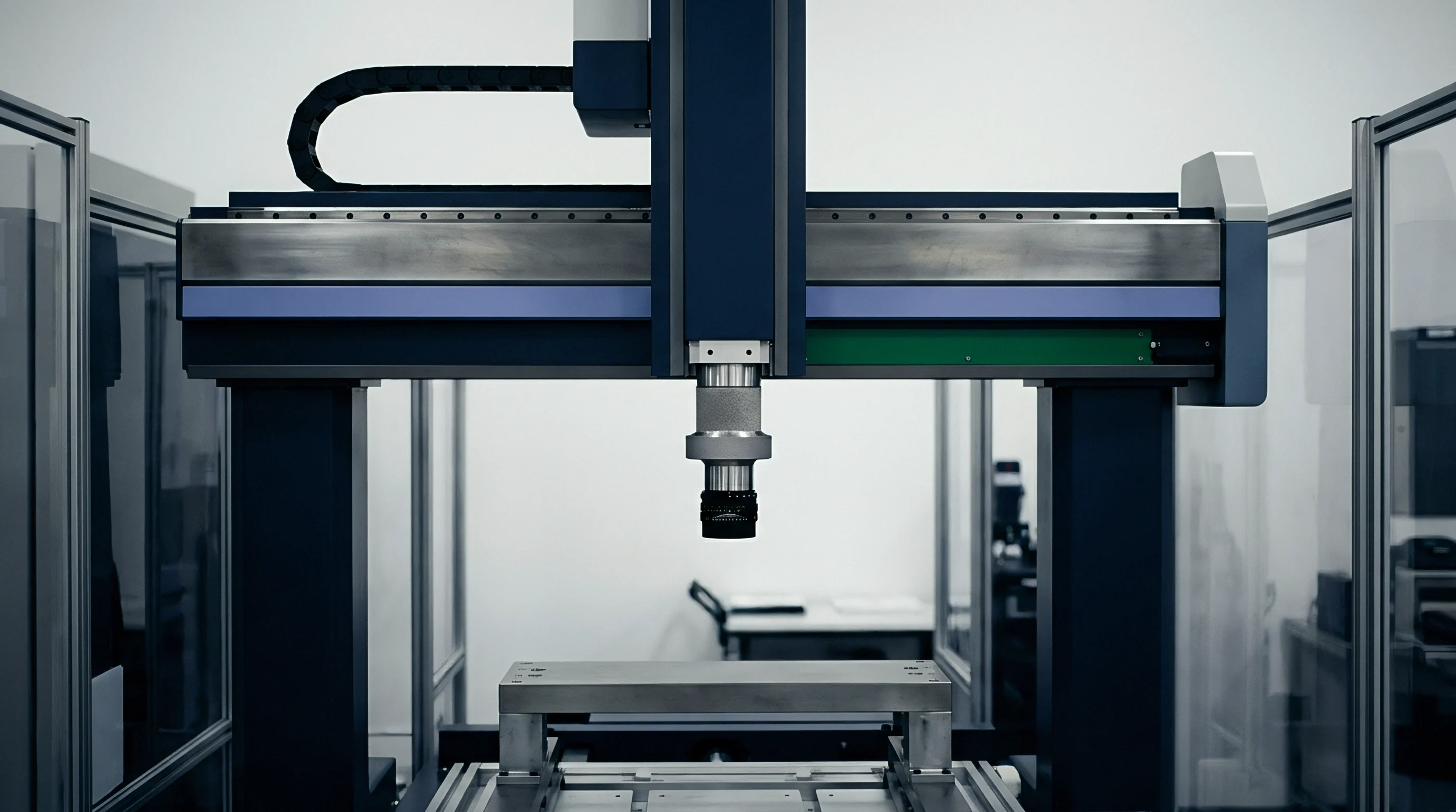
X-ray Fluorescence (XRF) analysis per ASTM B568 remains the standard non-destructive method for checking plating thickness and deposit composition. The instrument directs an incident X-ray beam at the busbar, knocking electrons out of the inner orbitals of coating and substrate atoms. As outer-shell electrons fall into the vacancies, they emit secondary fluorescent X-rays with energy peaks unique to each element.
Detectors measure the counts at these characteristic energy levels, and calibration software converts peak intensity into coating thickness and elemental ratios using absorption and emission models.
Multi-layer stacks require spectral deconvolution algorithms. When measuring tin over nickel on a copper base, the XRF spectrometer must resolve overlapping K-alpha and L-alpha emission lines for copper (8.04 keV), nickel (7.47 keV), and tin (25.27 keV). Secondary absorption, matrix effects, and spectral overlap require regular calibration against certified thin-film reference standards traceable to NIST or equivalent national metrology institutes.
Modern micro-focus XRF systems use polycapillary optics to concentrate the beam down to spot diameters under 30 micrometers, enabling thickness verification on tight bend radii, stamped steps, and laser weld zones.
Destructive metallographic cross-sectioning accompanied by Scanning Electron Microscopy (SEM) and Energy-Dispersive X-ray Spectroscopy (EDX) provides primary validation of XRF optical calibration curves. Cross-sectional preparation involves mounting cut busbar samples in epoxy resin, followed by mechanical grinding, diamond polishing down to 0.25-micrometer grit, and slight chemical etching to reveal interface boundaries. High-magnification SEM imaging visually resolves individual coating layer thicknesses down to 10-nanometer resolution, while EDX line scans profile chemical concentration gradients across the copper-nickel, nickel-tin, and tin-environment interfaces, resolving intermetallic compound composition and sub-surface voiding.
Is Automated X-Ray Fluorescence Sufficient For Batch Acceptance?
Relying exclusively on automated inline XRF thickness readings creates residual quality risks. Inline XRF spot checks verify coating depth at discrete locations but fail to detect sub-surface substrate oxidation, microscopic hydrogen pitting, or localized adhesion weaknesses. Implementing periodic destructive cross-sectional SEM-EDX testing alongside quantitative tape adhesion testing validates non-destructive XRF data, ensuring baseline structural integrity across volume production runs.
| Inspection Technology | Primary Parameter Measured | Measurement Resolution | Destructive Status | Standard Protocol |
|---|---|---|---|---|
| X-Ray Fluorescence (XRF) | Layer Thickness & Alloy Composition | 0.05 µm | Non-Destructive | ASTM B568 / ISO 3497 |
| Cross-Section SEM / EDX | Interface Morphology & IMC Growth | 10 nm | Destructive | ASTM B487 / ISO 1463 |
| Four-Point Micro-Ohm Meter | Interface Contact Resistance | 0.1 µΩ | Non-Destructive | MIL-STD-202 Method 307 |
| C-Mode Acoustic Microscopy | Sub-surface Delamination & Voids | 5.0 µm | Non-Destructive | IPC/JEDEC J-STD-035 |
Four-point micro-ohmmeter resistance testing measures joint contact quality without influence from test lead resistance. The instrument applies a known direct current (I) through outer current probes while dedicated inner voltage probes measure the voltage drop (V) across the plated interface. Applying low currents prevents heating effects that alter material resistivity during measurement.
Comparing joint resistance before and after environmental exposure provides a quantitative metric of surface degradation, oxidation growth, and fretting wear within bolted busbar joints.
Optical surface profilometry provides non-contact 3D mapping of plating roughness and surface topographies. White-light interferometry (WLI) and confocal laser scanning microscopy capture surface heights with sub-nanometer vertical resolution across millimeter-scale field areas. 3D surface parameters, such as areal surface roughness (Sa) and peak extreme height (Sxp), characterize surface topography better than 2D line profiles, enabling accurate prediction of contact area dynamics and seal compression performance in IP67-rated pack enclosures.
Consider a post-mortem analysis of high-voltage battery pack failures operating under high humidity conditions. An automotive pack design specified a minimum nickel underlayer thickness of 3.0 micrometers beneath 5.0 micrometers of matte tin across a copper busbar. Routine inline XRF inspection reported compliant tin thickness averaging 5.2 micrometers.
Field returns exhibited severe galvanic pitting and localized joint overheating within 18 months of service. Metallographic cross-sectioning and EDX line scans revealed that the inline XRF instrument was incorrectly calibrated for single-layer tin over copper, mistaking the total spectrum count for tin and masking a complete absence of the nickel barrier layer due to plating tank chemical exhaustion. The unbarriered tin allowed rapid copper diffusion, generating a 4.0-micrometer thick brittle Cu6Sn5 intermetallic layer that fractured under thermal cycling, exposing bare copper to ambient condensation.
Recalibrating metrology equipment to mandate multi-layer deconvolution routines and pairing non-destructive XRF screening with weekly destructive cross-sectional SEM audits prevents unbarriered parts from entering assembly operations.
Scanning Acoustic Microscopy (C-SAM) utilizes high-frequency focused ultrasound (20 MHz to 230 MHz) to detect internal sub-surface delamination, micro-voids, and inclusions within plated busbar stacks. Ultrasonic pulses reflect off internal material interfaces where acoustic impedance changes occur. Delamination voids between nickel plating and copper substrates cause complete reflection of sound waves, producing high-contrast acoustic images of sub-surface unbonded areas.
Non-destructive acoustic screening enables 100 percent inspection of critical busbar components intended for aerospace or ultra-high-reliability energy storage applications.
What structural anomalies remain undetected when metrology protocols rely solely on surface roughness measurements without monitoring subsurface intermetallic phase growth?
Sampling
Statistical Quality Control (SQC) frameworks govern lot acceptance, verification frequency, and sampling plans for incoming plated busbars. High-volume battery manufacturing lines cannot perform 100 percent destructive adhesion or cross-sectional thickness testing without destroying production yield and inflating unit costs. Standardized acceptance sampling plans per ISO 2859-1 (ANSI/ASQ Z1.4) establish statistically sound sample sizes (n) and acceptance thresholds (c) based on total lot size (N) and designated Acceptable Quality Limits (AQL).
Zero Acceptance Number (C=0) sampling plans per Squeglia standards replace traditional AQL attribute sampling in critical automotive power-train applications. Under traditional AQL plans, sample lots permit a small number of defective units (c ge 1) while still passing the entire shipment. C=0 sampling plans dictate that if a single non-conforming sample unit is detected within the drawn sample size (n), the entire production lot fails inspection immediately.
For safety-critical busbar components where plating failure leads to thermal runaway, engineering teams enforce C=0 sampling with strict sample size selection based on lot risk categorizations.
Sampling plans distinguish non-destructive dimensional and surface checks from destructive mechanical and chemical verification tests. Non-destructive tests, such as visual inspection, surface roughness profiling, and XRF thickness spot checks, utilize Normal Inspection Level II under ISO 2859-1. Destructive tests, such as cross-hatch tape adhesion, thermal shock cycling, and cross-sectional SEM-EDX measurement, follow Special Inspection Levels S-2 or S-3 to minimize material loss while maintaining statistical control confidence limits exceeding 95 percent.
| Verification Parameter | Inspection Standard | Sampling Level / Plan | Acceptance Criteria (AQL / C=0) | Test Action Required |
|---|---|---|---|---|
| Visual & Surface Defects | ISO 2859-1 Level II | Normal Single (n=125 for N=10k) | AQL 0.40 (c=1) | Non-Destructive Visual 10x |
| XRF Coating Thickness | ASTM B568 | C=0 Plan (n=32 for N=10k) | C=0 (0 Defects Allowed) | Non-Destructive 5-Point Check |
| Cross-Hatch Adhesion | ASTM D3359 | Level S-3 (n=8 for N=10k) | C=0 (5B Rating Required) | Destructive Cut & Tape Pull |
| Salt Spray Resistance | ISO 9227 / ASTM B117 | Level S-2 (n=5 per Lot) | C=0 (Zero Base Metal Rust) | Destructive 240h Exposure |
Statistical process control (SPC) relies on continuous calculation of process capability metrics, specifically Cp and Cpk. The process capability index (Cpk) accounts for process mean shifts relative to double-sided engineering tolerance specification limits (Upper Specification Limit USL and Lower Specification Limit LSL):
Cpk = minleft( fracUSL – μ3σ, fracμ – LSL3σ right)
A Cpk index of 1.33 indicates acceptable process control (four-sigma quality level), while automotive power-train specifications mandate a minimum Cpk of 1.67 (five-sigma quality level) for critical plating thickness attributes. When SPC control charts indicate process mean shifts or Cpk values dropping below 1.33, the manufacturing execution system (MES) triggers automated tool holds and mandates immediate bath chemical titration adjustments.
Comprehensive traceability protocols link physical busbar lots directly to electroplating line parameters. Automated manufacturing lines apply unique 2D DataMatrix codes via fiber laser marking directly onto raw copper busbars prior to plating pre-treatment. Matrix codes store part identity, raw material melt heat numbers, plating line identification, chemical bath lot numbers, electrodeposition rack coordinates, and timestamped process data (current density, bath temperature, pH, and line speed).
Full digital traceability ensures that if a field failure occurs, quality engineers can trace and isolate affected serial numbers across supply chains.
Supplier lot certification documentation must accompany every incoming component shipment. Quality agreements require suppliers to provide a formal Certificate of Analysis (CoA) containing real-time XRF thickness distributions, SPC control chart data (Cpk outputs), adhesion test verification logs, and raw material chemical assay reports. Quality teams audit supplier manufacturing facilities annually, validating bath titration frequency, laboratory instrument calibration records, and process control compliance.
Incoming inspection procedures require immediate quarantine of shipments failing initial verification checks. When a sample unit fails XRF thickness, cross-hatch adhesion, or surface cleanliness checks, quality teams issue a Supplier Corrective Action Request (SCAR) and freeze the entire lot in the warehouse MES environment. The plating supplier must execute root-cause analysis using 8D methodology, identify process lapses, rectify bath parameters, and submit verified replacement lots before warehouse releases occur.
The statistical sampling and quality verification workflow mandates structured execution phases across incoming batch lots:
- Lot Registration scans incoming DataMatrix codes to enter shipment volume into the warehouse inventory system.
- Attribute Inspection extracts non-destructive sample sizes per ISO 2859-1 Level II to evaluate surface defects, dimensional tolerances, and surface roughness parameters.
- XRF Screening executes five-point thickness measurements across critical contact pads and flexure radii using calibrated micro-focus X-ray systems.
- Destructive Verification pulls sub-samples per Level S-3 for cross-hatch adhesion testing, solderability checks, and micro-bend ductility evaluation.
- Data Logging inputs physical inspection records into the SPC database to recalculate real-time supplier Cpk trend curves.
- Warehouse Quarantine Release transfers approved material directly into line inventory or routes non-conforming lots to quarantine storage.
Receiving inspection teams log material test records into centralized enterprise systems before releasing parts to production line locations. This verification barrier ensures that non-conforming plating runs cannot enter pack assembly operations.

Warranty
Technical specifications embedded within commercial supply contracts define legal liability, financial exposure, and warranty boundaries across the energy storage supply chain. When field failures occur due to joint resistance elevation, thermal runaway propagation, or plating degradation, contractual language determines whether cost recovery rests with the cell supplier, electroplating vendor, pack integrator, or automotive original equipment manufacturer (OEM). Explicit engineering drawings and verification standards form the primary baseline for legal liability arbitration.
Clear demarcation of engineering responsibility relies on unambiguous drawings and referenced verification standards. General notes such as “plating must be continuous and free of defects” hold zero legal enforceability during warranty disputes. Purchase specifications mandate exact, measurable attributes: minimum and maximum layer thickness tolerances, micro-hardness ranges, allowable surface roughness (Ra limits), required adhesion performance per ASTM D3359, and exact salt spray exposure hours per ISO 9227 without base metal corrosion.
Incorporating quantitative metrics into contract drawings establishes clear pass/fail legal boundaries during formal dispute resolution.
Quality agreements mandate supplier compliance with formal Advanced Product Quality Planning (APQP) and Production Part Approval Process (PPAP) frameworks per IATF 16949 standards. Level 3 PPAP submission packages demand complete disclosure of electroplating process flow diagrams, Process Failure Mode and Effects Analysis (PFMEA), Control Plans, Measurement System Analysis (MSA) studies for XRF equipment, and full First Article Inspection (FAI) reports. Once an OEM approves a supplier PPAP submission, the electroplating vendor cannot alter chemical bath suppliers, line speed, pre-treatment acid concentrations, or plating thickness limits without formal Engineering Change Request (ECR) submission and written customer authorization.
Commercial warranty risk distribution depends on precise contractual liability allocation clauses:
- Direct Financial Recourse mandates that plating vendors absorb total field recall costs, including labor and pack replacement fees, if failures stem from undocumented PPAP process deviations.
- Warranty Seam Definition establishes clear boundaries dividing cell terminal welding defects from supplier plating adhesion failures based on cross-sectional SEM analysis.
- Capped Liability Provisions restrict supplier financial exposure to a fixed multiple of annual contract purchase value in exchange for strict lot quarantine protocols.
- Serial Failure Triggers define automatic contract termination and lot rejection parameters when batch failure rates exceed 0.05 percent over consecutive quarters.
Unannounced process modifications by electroplating vendors represent a major source of field warranty claims. Suppliers facing rising material costs may attempt to trim gold or silver flash thickness, switch from electroless nickel to cheaper electrolytic baths, or extend chemical bath usage past recommended bath life limits. These unapproved process modifications alter internal layer stress profiles and corrosion resistance without changing initial visual appearance.
Quality agreements enforce heavy financial indemnification penalties and immediate vendor disqualified status if audits reveal unauthorized chemistry modifications.
Insurance underwriters and financial institutions require verified compliance documentation before extending product liability coverage for large-scale grid energy storage installations. Standard verification dossiers must contain certified third-party laboratory test reports validating plating performance against long-term environmental degradation, thermal cycling strain, and salt fog immersion. Complete testing documentation lowers insurance premiums and simplifies project debt financing by establishing rigorous engineering risk management.
Technical specifications write exact failure allocation protocols into long-term supply agreements. When joint failure occurs in the field, independent accredited laboratories perform metallographic cross-sectioning, micro-hardness mapping, and EDX elemental analysis on failed busbar samples to establish root cause and assign contractual liability.